
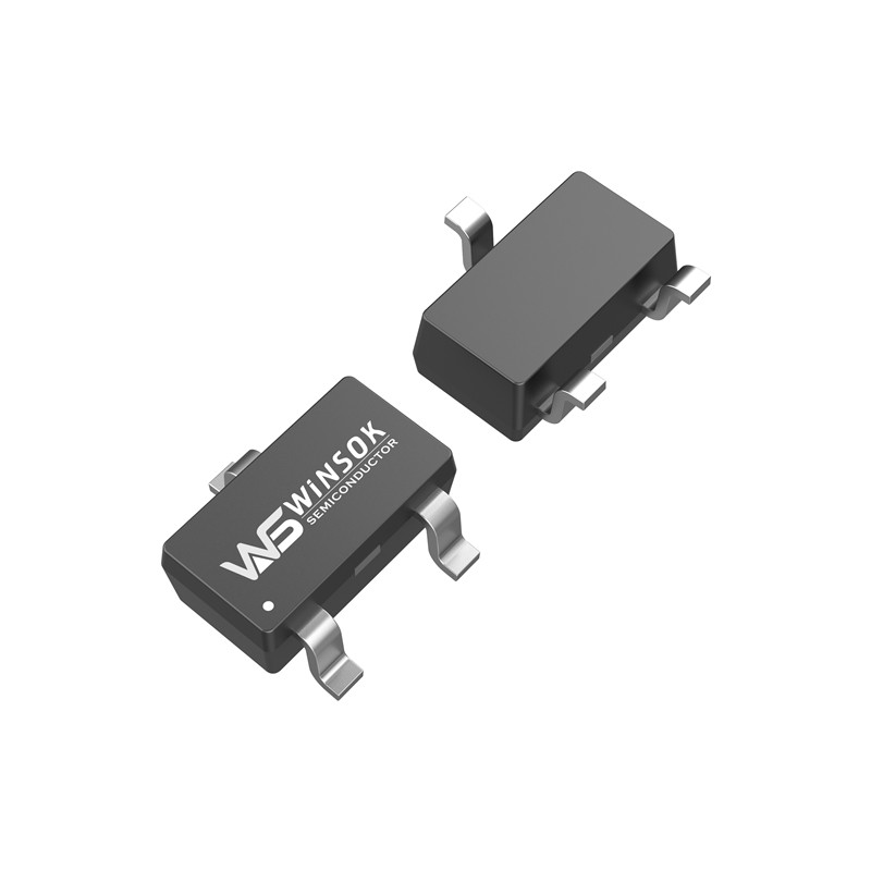
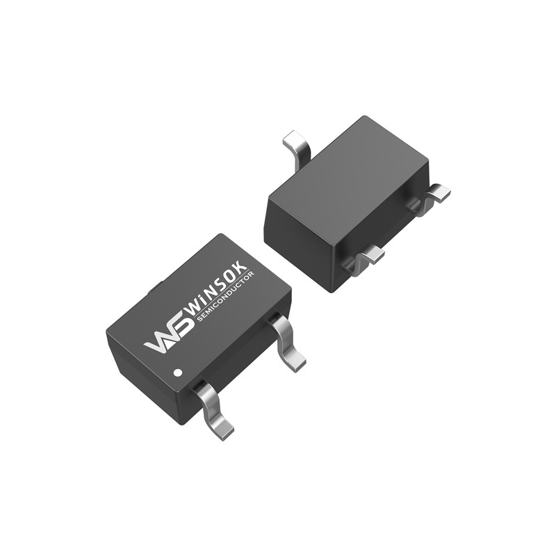
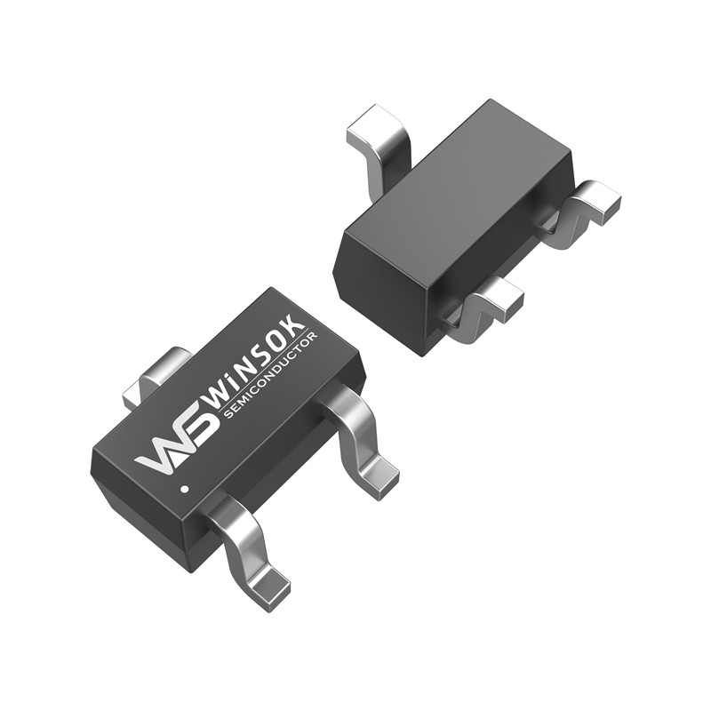
WST4041 P-Channel -40V -6A SOT-23-3L WINSOK MOSFET
General Description
The WST4041 is a powerful P-channel MOSFET designed for use in synchronous buck converters. It has a high cell density that allows for excellent RDSON and gate charge. The WST4041 meets requirements for RoHS and Green Product standards, and it comes with a 100% EAS guarantee for reliable performance.
Features
Advanced Trench Technology features high cell density and super low gate charge, significantly reducing the CdV/dt effect. Our devices come with a 100% EAS guarantee and environmentally friendly options.
Applications
High-frequency point-of-load synchronous buck converter, networking DC-DC power system, load switch, e-cigarettes, controllers, digital devices, small home appliances, and consumer electronics.
corresponding material number
AOS AO3409 AOS3403 AOS3421 AOS3421E AO3401 AOS3401A,dintek DTS4501,ncepower NCE40P05Y,
Important parameters
| Symbol | Parameter | Rating | Units |
| VDS | Drain-Source Voltage | -40 | V |
| VGS | Gate-Source Voltage | ±20 | V |
| ID@TC=25℃ | Continuous Drain Current, VGS @ -10V1 | -6.0 | A |
| ID@TC=100℃ | Continuous Drain Current, VGS @ -10V1 | -4.5 | A |
| IDM | Pulsed Drain Current2 | -24 | A |
| EAS | Single Pulse Avalanche Energy3 | 12 | mJ |
| IAS | Avalanche Current | -7 | A |
| PD@TC=25℃ | Total Power Dissipation4 | 1.4 | W |
| TSTG | Storage Temperature Range | -55 to 150 | ℃ |
| TJ | Operating Junction Temperature Range | -55 to 150 | ℃ |
| Symbol | Parameter | Conditions | Min. | Typ. | Max. | Unit |
| BVDSS | Drain-Source Breakdown Voltage | VGS=0V , ID=-250uA | -40 | --- | --- | V |
| △BVDSS/△TJ | BVDSS Temperature Coefficient | Reference to 25℃ , ID=-1mA | --- | -0.03 | --- | V/℃ |
| RDS(ON) | Static Drain-Source On-Resistance2 | VGS=-10V , ID=-3A | --- | 30 | 40 | mΩ |
| VGS=-4.5V , ID=-1A | --- | 40 | 58 | |||
| VGS(th) | Gate Threshold Voltage | VGS=VDS , ID =-250uA | -0.8 | -1.2 | -2.2 | V |
| △VGS(th) | VGS(th) Temperature Coefficient | --- | 4.56 | --- | mV/℃ | |
| IDSS | Drain-Source Leakage Current | VDS=-28V , VGS=0V , TJ=25℃ | --- | --- | 1 | uA |
| VDS=-28V , VGS=0V , TJ=55℃ | --- | --- | 5 | |||
| IGSS | Gate-Source Leakage Current | VGS=±20V , VDS=0V | --- | --- | ±100 | nA |
| gfs | Forward Transconductance | VDS=-5V , ID=-3A | --- | 15 | --- | S |
| Rg | Gate Resistance | VDS=0V , VGS=0V , f=1MHz | --- | 3.8 | --- | Ω |
| Qg | Total Gate Charge (-4.5V) | VDS=-18V , VGS=-10V , ID=-4A | --- | 9.5 | --- | nC |
| Qgs | Gate-Source Charge | --- | 1.7 | --- | ||
| Qgd | Gate-Drain Charge | --- | 2.0 | --- | ||
| Td(on) | Turn-On Delay Time | VDD=-15V , VGS=-10V ,
RG=6Ω, ID=-1A , RL=15Ω |
--- | 8 | --- | ns |
| Tr | Rise Time | --- | 10 | --- | ||
| Td(off) | Turn-Off Delay Time | --- | 18 | --- | ||
| Tf | Fall Time | --- | 8 | --- | ||
| Ciss | Input Capacitance | VDS=-15V , VGS=0V , f=1MHz | --- | 420 | --- | pF |
| Coss | Output Capacitance | --- | 77 | --- | ||
| Crss | Reverse Transfer Capacitance | --- | 55 | --- |
Why Choose Us?
Better Than Factory Prices
Competitive pricing that beats direct factory offers through our strategic partnerships
Fast Shipping
Large inventory ready for immediate dispatch with quick delivery times
Premium Service
Superior customer support and technical assistance throughout your journey
FAQ
How to Place an Order?
1. Submit inquiry through our website
2. Receive quotation within 24 hours
3. Confirm order details and make payment
4. Order processing and shipping
MOQ & Payment Terms
• Standard MOQ: 1000 pieces
• Sample order: 10-50 pieces
• Payment Terms: 30% deposit, 70% before shipment
Payment Methods
• T/T (Bank Transfer)
• Letter of Credit (L/C)
• Western Union
• PayPal (for sample orders)
Shipping & Delivery
• Warehouses: Hong Kong & Shenzhen
• Delivery time: 3-5 days after payment
• Express services: DHL, FedEx, UPS
• Air freight available for bulk orders
Certifications & Quality Assurance

ISO 9001:2015
Quality Management System Certified

RoHS Compliant
Environmental Protection Standard

REACH Compliant
European Union Safety Standard
Customer Testimonials
Real feedback from our global customers, witnessing our quality and service excellence

Olukey's MOSFETs consistently deliver stable quality with precise delivery times. We've made multiple purchases and remain highly satisfied.
Procurement Manager @ XYZ Electronics (India)

Competitive pricing coupled with responsive technical support helped us optimize our circuit design effectively.
Supply Chain Executive @ TechPower Solutions (Vietnam)

From small batch testing to mass production, our cooperation has been seamless. A truly reliable long-term partner.
Hardware Engineer @ BrightCircuit Innovations (Malaysia)
Our Trusted Partners
Our products are successfully implemented in smart devices, power adapters, and industrial equipment by global brands


📌Choose Olukey for a More Efficient and Reliable Supply Chain!
-

WSD2068DN23 WSD2098DN23 Dual N-Ch -20V 7.5A DFN...
-

WSK150N12 N-channel 120V 150A TO-263-2L WINSOK ...
-

WST2N7002 N-channel 60V 0.18A SOT-23L WINSOK MO...
-

WSR180N10 N-channel 100V 180A TO-220-3L WINSOK ...
-
WST3424 WST3420 WST2300 WST2304 N-channel 20V 6...
-

WSP4016 N-channel 40V 15.5A SOP-8 WINSOK MOSFET


