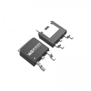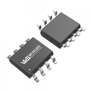
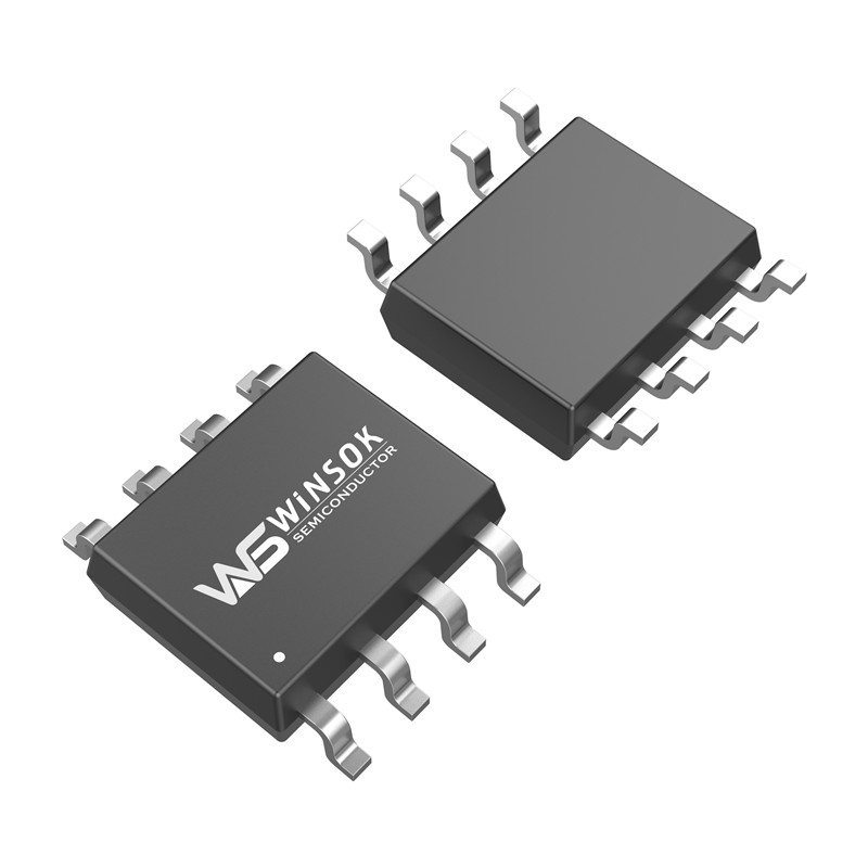
WSP4447 P-Channel -40V -11A SOP-8 WINSOK MOSFET
General Description
The WSP4447 is a top-performing MOSFET that utilizes trench technology and has a high cell density. It offers excellent RDSON and gate charge, making it suitable for use in most synchronous buck converter applications. The WSP4447 meets RoHS and Green Product standards, and comes with 100% EAS guarantee for full reliability.
Features
Advanced Trench technology allows for higher cell density, resulting in a Green Device with Super Low Gate Charge and excellent CdV/dt effect decline.
Applications
High Frequency Converter for a Variety of Electronics
This converter is designed to efficiently power a wide range of devices, including laptops, gaming consoles, networking equipment, e-cigarettes, wireless chargers, motors, drones, medical devices, car chargers, controllers, digital products, small home appliances, and consumer electronics.
corresponding material number
AOS AO4425 AO4485,ON FDS4675,VISHAY Si4401FDY,ST STS10P4LLF6,TOSHIBA TPC8133,PANJIT PJL9421,Sinopower SM4403PSK,RUICHIPS RU40L10H.
Important parameters
| Symbol | Parameter | Rating | Units |
| VDS | Drain-Source Voltage | -40 | V |
| VGS | Gate-Source Voltage | ±20 | V |
| ID@TA=25℃ | Continuous Drain Current, VGS @ -10V1 | -11 | A |
| ID@TA=70℃ | Continuous Drain Current, VGS @ -10V1 | -9.0 | A |
| IDM a | 300µs Pulsed Drain Current (VGS=-10V) | -44 | A |
| EAS b | Avalanche Energy, Single pulse (L=0.1mH) | 54 | mJ |
| IAS b | Avalanche Current, Single pulse (L=0.1mH) | -33 | A |
| PD@TA=25℃ | Total Power Dissipation4 | 2.0 | W |
| TSTG | Storage Temperature Range | -55 to 150 | ℃ |
| TJ | Operating Junction Temperature Range | -55 to 150 | ℃ |
| Symbol | Parameter | Conditions | Min. | Typ. | Max. | Unit |
| BVDSS | Drain-Source Breakdown Voltage | VGS=0V , ID=-250uA | -40 | --- | --- | V |
| △BVDSS/△TJ | BVDSS Temperature Coefficient | Reference to 25℃ , ID=-1mA | --- | -0.018 | --- | V/℃ |
| RDS(ON) | Static Drain-Source On-Resistance2 | VGS=-10V , ID=-13A | --- | 13 | 16 | mΩ |
| VGS=-4.5V , ID=-5A | --- | 18 | 26 | |||
| VGS(th) | Gate Threshold Voltage | VGS=VDS , ID =-250uA | -1.4 | -1.9 | -2.4 | V |
| △VGS(th) | VGS(th) Temperature Coefficient | --- | 5.04 | --- | mV/℃ | |
| IDSS | Drain-Source Leakage Current | VDS=-32V , VGS=0V , TJ=25℃ | --- | --- | -1 | uA |
| VDS=-32V , VGS=0V , TJ=55℃ | --- | --- | -5 | |||
| IGSS | Gate-Source Leakage Current | VGS=±20V , VDS=0V | --- | --- | ±100 | nA |
| gfs | Forward Transconductance | VDS=-5V , ID=-10A | --- | 18 | --- | S |
| Qg | Total Gate Charge (-4.5V) | VDS=-20V , VGS=-10V , ID=-11A | --- | 32 | --- | nC |
| Qgs | Gate-Source Charge | --- | 5.2 | --- | ||
| Qgd | Gate-Drain Charge | --- | 8 | --- | ||
| Td(on) | Turn-On Delay Time | VDD=-20V , VGS=-10V ,
RG=6Ω, ID=-1A ,RL=20Ω |
--- | 14 | --- | ns |
| Tr | Rise Time | --- | 12 | --- | ||
| Td(off) | Turn-Off Delay Time | --- | 41 | --- | ||
| Tf | Fall Time | --- | 22 | --- | ||
| Ciss | Input Capacitance | VDS=-15V , VGS=0V , f=1MHz | --- | 1500 | --- | pF |
| Coss | Output Capacitance | --- | 235 | --- | ||
| Crss | Reverse Transfer Capacitance | --- | 180 | --- |
Why Choose Us?
Better Than Factory Prices
Competitive pricing that beats direct factory offers through our strategic partnerships
Fast Shipping
Large inventory ready for immediate dispatch with quick delivery times
Premium Service
Superior customer support and technical assistance throughout your journey
FAQ
How to Place an Order?
1. Submit inquiry through our website
2. Receive quotation within 24 hours
3. Confirm order details and make payment
4. Order processing and shipping
MOQ & Payment Terms
• Standard MOQ: 1000 pieces
• Sample order: 10-50 pieces
• Payment Terms: 30% deposit, 70% before shipment
Payment Methods
• T/T (Bank Transfer)
• Letter of Credit (L/C)
• Western Union
• PayPal (for sample orders)
Shipping & Delivery
• Warehouses: Hong Kong & Shenzhen
• Delivery time: 3-5 days after payment
• Express services: DHL, FedEx, UPS
• Air freight available for bulk orders
Certifications & Quality Assurance

ISO 9001:2015
Quality Management System Certified

RoHS Compliant
Environmental Protection Standard

REACH Compliant
European Union Safety Standard
Customer Testimonials
Real feedback from our global customers, witnessing our quality and service excellence

Olukey's MOSFETs consistently deliver stable quality with precise delivery times. We've made multiple purchases and remain highly satisfied.
Procurement Manager @ XYZ Electronics (India)

Competitive pricing coupled with responsive technical support helped us optimize our circuit design effectively.
Supply Chain Executive @ TechPower Solutions (Vietnam)

From small batch testing to mass production, our cooperation has been seamless. A truly reliable long-term partner.
Hardware Engineer @ BrightCircuit Innovations (Malaysia)
Our Trusted Partners
Our products are successfully implemented in smart devices, power adapters, and industrial equipment by global brands


📌Choose Olukey for a More Efficient and Reliable Supply Chain!