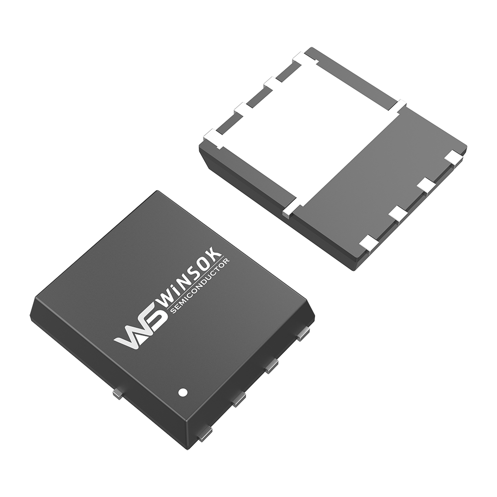
WSD6070DN56 N-channel 60V 80A DFN5X6-8 WINSOK MOSFET
WINSOK MOSFET product overview
The voltage of WSD6070DN56 MOSFET is 60V, the current is 80A, the resistance is 7.3mΩ, the channel is N-channel, and the package is DFN5X6-8.
WINSOK MOSFET application areas
E-cigarettes MOSFET, wireless charging MOSFET, motors MOSFET, drones MOSFET, medical care MOSFET, car chargers MOSFET, controllers MOSFET, digital products MOSFET, small household appliances MOSFET, consumer electronics MOSFET.
WINSOK MOSFET corresponds to other brand material numbers
POTENS Semiconductor MOSFET PDC696X.
MOSFET parameters
|
Symbol |
Parameter |
Rating |
Units |
|
VDS |
Drain-Source Voltage |
60 |
V |
|
VGS |
Gate-Source Voltage |
±20 |
V |
|
TJ |
Maximum Junction Temperature |
150 |
°C |
|
ID |
Storage Temperature Range |
-55 to 150 |
°C |
|
IS |
Diode Continuous Forward Current,TC=25°C |
80 |
A |
|
ID |
Continuous Drain Current, VGS=10V,TC=25°C |
80 |
A |
| Continuous Drain Current, VGS=10V,TC=100°C |
66 |
A |
|
|
IDM |
Pulsed Drain Current ,TC=25°C |
300 |
A |
|
PD |
Maximum Power Dissipation,TC=25°C |
150 |
W |
| Maximum Power Dissipation,TC=100°C |
75 |
W |
|
|
RθJA |
Thermal Resistance-Junction to Ambient ,t =10s ̀ |
50 |
°C/W |
|
Thermal Resistance-Junction to Ambient ,Steady State |
62.5 |
°C/W |
|
|
RqJC |
Thermal Resistance-Junction to Case |
1 |
°C/W |
|
IAS |
Avalanche Current, Single pulse,L=0.5mH |
30 |
A |
|
EAS |
Avalanche Energy, Single pulse,L=0.5mH |
225 |
mJ |
|
Symbol |
Parameter |
Conditions |
Min. |
Typ. |
Max. |
Unit |
|
BVDSS |
Drain-Source Breakdown Voltage | VGS=0V , ID=250uA |
60 |
--- |
--- |
V |
|
△BVDSS/△TJ |
BVDSS Temperature Coefficient | Reference to 25℃ , ID=1mA |
--- |
0.043 |
--- |
V/℃ |
|
RDS(ON) |
Static Drain-Source On-Resistance2 | VGS=10V , ID=40A |
--- |
7.0 |
9.0 |
mΩ |
|
VGS(th) |
Gate Threshold Voltage | VGS=VDS , ID =250uA |
2.0 |
3.0 |
4.0 |
V |
|
△VGS(th) |
VGS(th) Temperature Coefficient |
--- |
-6.94 |
--- |
mV/℃ | |
|
IDSS |
Drain-Source Leakage Current | VDS=48V , VGS=0V , TJ=25℃ |
--- |
--- |
2 |
uA |
| VDS=48V , VGS=0V , TJ=55℃ |
--- |
--- |
10 |
|||
|
IGSS |
Gate-Source Leakage Current | VGS=±20V , VDS=0V |
--- |
--- |
±100 |
nA |
|
gfs |
Forward Transconductance | VDS=5V , ID=20A |
--- |
50 |
--- |
S |
|
Rg |
Gate Resistance | VDS=0V , VGS=0V , f=1MHz |
--- |
1.0 |
--- |
Ω |
|
Qg |
Total Gate Charge (10V) | VDS=30V , VGS=10V , ID=40A |
--- |
48 |
--- |
nC |
|
Qgs |
Gate-Source Charge |
--- |
17 |
--- |
||
|
Qgd |
Gate-Drain Charge |
--- |
12 |
--- |
||
|
Td(on) |
Turn-On Delay Time | VDD=30V , VGEN=10V , RG=1Ω, ID=1A ,RL=15Ω. |
--- |
16 |
--- |
ns |
|
Tr |
Rise Time |
--- |
10 |
--- |
||
|
Td(off) |
Turn-Off Delay Time |
--- |
40 |
--- |
||
|
Tf |
Fall Time |
--- |
35 |
--- |
||
|
Ciss |
Input Capacitance | VDS=30V , VGS=0V , f=1MHz |
--- |
2680 |
--- |
pF |
|
Coss |
Output Capacitance |
--- |
386 |
--- |
||
|
Crss |
Reverse Transfer Capacitance |
--- |
160 |
--- |
Why Choose Us?
Better Than Factory Prices
Competitive pricing that beats direct factory offers through our strategic partnerships
Fast Shipping
Large inventory ready for immediate dispatch with quick delivery times
Premium Service
Superior customer support and technical assistance throughout your journey
FAQ
How to Place an Order?
1. Submit inquiry through our website
2. Receive quotation within 24 hours
3. Confirm order details and make payment
4. Order processing and shipping
MOQ & Payment Terms
• Standard MOQ: 1000 pieces
• Sample order: 10-50 pieces
• Payment Terms: 30% deposit, 70% before shipment
Payment Methods
• T/T (Bank Transfer)
• Letter of Credit (L/C)
• Western Union
• PayPal (for sample orders)
Shipping & Delivery
• Warehouses: Hong Kong & Shenzhen
• Delivery time: 3-5 days after payment
• Express services: DHL, FedEx, UPS
• Air freight available for bulk orders
Certifications & Quality Assurance

ISO 9001:2015
Quality Management System Certified

RoHS Compliant
Environmental Protection Standard

REACH Compliant
European Union Safety Standard
Customer Testimonials
Real feedback from our global customers, witnessing our quality and service excellence

Olukey's MOSFETs consistently deliver stable quality with precise delivery times. We've made multiple purchases and remain highly satisfied.
Procurement Manager @ XYZ Electronics (India)

Competitive pricing coupled with responsive technical support helped us optimize our circuit design effectively.
Supply Chain Executive @ TechPower Solutions (Vietnam)

From small batch testing to mass production, our cooperation has been seamless. A truly reliable long-term partner.
Hardware Engineer @ BrightCircuit Innovations (Malaysia)
Our Trusted Partners
Our products are successfully implemented in smart devices, power adapters, and industrial equipment by global brands


📌Choose Olukey for a More Efficient and Reliable Supply Chain!