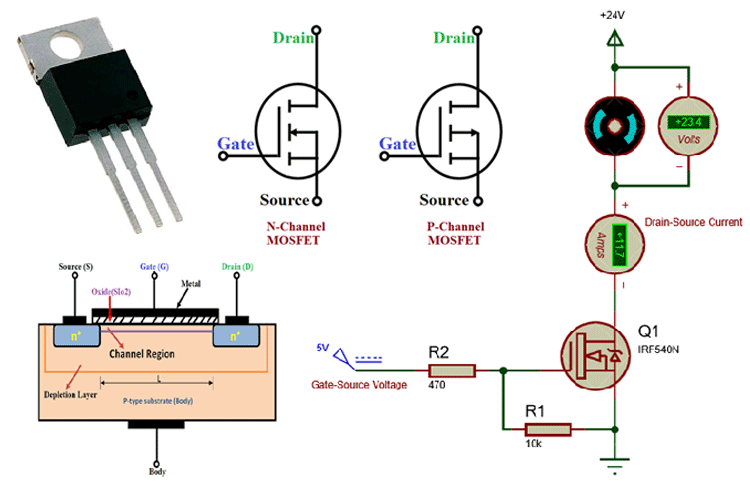
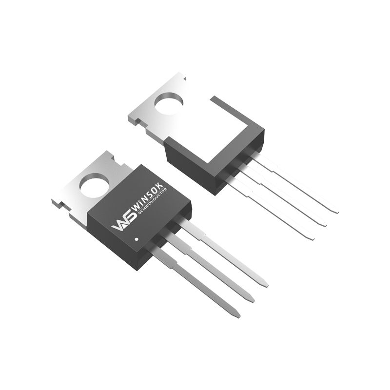
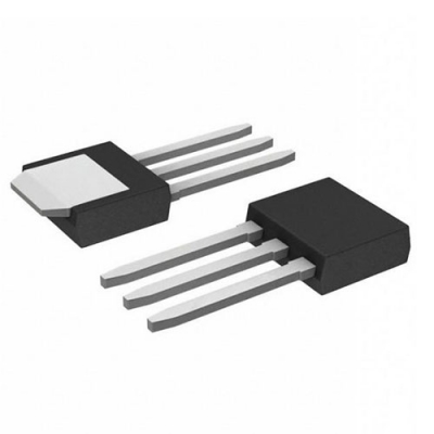
MOSFET Structure and Pin Configuration
 This packaged MOSFET pyroelectric infrared sensor features a distinctive rectangular frame serving as the sensing window. The device incorporates three essential pins:
- • G pin (Ground terminal)
- • D pin (Internal MOSFET drain)
- • S pin (Internal MOSFET source)
In practical circuit applications, G connects to ground, D links to the positive power supply, while infrared signals enter through the window and electrical signals output via S.
MOS Driver and Gate Characteristics
The MOS driver plays a crucial role in waveform shaping and driving enhancement. A suboptimal G signal waveform lacking sufficient steepness can result in substantial power loss during switching stages. This inefficiency manifests in:
- • Reduced circuit conversion efficiency
- • Excessive heat generation in the MOSFET
- • Potential thermal damage
The presence of capacitance between MOSFET GS necessitates adequate G signal driving capability to prevent compromised waveform jump time.
Testing Procedures
Gate (G) Identification:
Short-circuit the G-S pole and use a multimeter set to R×1 level. Connect the black test lead to S and red to D. Expected resistance: few Ω to >10 Ω. The G pole is confirmed when infinite resistance is measured between it and other pins, regardless of lead polarity.
Source (S) and Drain (D) Identification:
Using R×1k setting, measure inter-pin resistance twice with exchanged leads. The lower resistance value (typically few kΩ to >10 kΩ) indicates forward resistance. Black lead identifies S pole, red indicates D pole.
MOSFET Types and Principles
MOSFETs come in two primary variants:
- • N-channel MOSFET (NMOS)
- • P-channel MOSFET (PMOS) - featuring lightly doped N-type backgate with P-type source and drain
Both variants operate on the fundamental principle of voltage-controlled current regulation. The gate voltage controls drain current output, distinguishing MOSFETs from traditional transistors by eliminating base current-induced charge storage effects. This results in superior switching speeds.
Technical Foundation
The Field Effect Transistor (FET) derives its name from the electric field projection through an insulating layer, controlling current flow. The gate's minimal current flow through this insulator results in extremely low gate current.
Modern MOSFETs typically employ silicon dioxide as the gate insulator, earning the "metal oxide semiconductor" designation. Their compact size and energy efficiency have made them the preferred choice over bipolar transistors in numerous applications.
Advanced Applications and Industry Trends
 MOSFETs have become integral components in modern electronics, finding applications across diverse sectors:
Power Management
In switching power supplies and voltage regulators, MOSFETs excel at high-frequency switching applications, enabling:
- • Efficient DC-DC conversion
- • Power factor correction
- • Battery management systems
Automotive Electronics
The automotive industry increasingly relies on MOSFETs for:
- • Electric vehicle power systems
- • Motor controllers
- • LED lighting control
- • Battery protection circuits
Selection Considerations
When choosing MOSFETs for specific applications, several key parameters require careful consideration:
- • VDS (Drain-Source Voltage): Maximum voltage the MOSFET can block
- • RDS(on): Drain-source on-state resistance, crucial for power efficiency
- • ID: Maximum continuous drain current capability
- • Gate Charge (Qg): Affects switching speed and drive requirements
Future Developments
The MOSFET industry continues to evolve with emerging technologies:
- • Wide-bandgap semiconductors (SiC and GaN)
- • Advanced packaging techniques for better thermal performance
- • Integration with smart protection features
- • Improved efficiency for high-frequency applications
Design Considerations
Optimal MOSFET implementation requires attention to:
- • Thermal management strategies
- • PCB layout optimization
- • Gate drive circuit design
- • Protection against voltage transients
Industry Standards and Reliability
Modern MOSFETs are manufactured to meet stringent industry standards:
- • AEC-Q101 qualification for automotive applications
- • RoHS compliance for environmental safety
- • Enhanced ESD protection capabilities
- • Improved avalanche energy ratings
Premium MOSFET Solutions from Olukey
As the authorized distributor for Winsok, Taiwan's leading MOSFET manufacturer, we provide:
- ✓ Comprehensive range of high-performance MOSFETs
- ✓ Professional technical support and consultation
- ✓ Authentic products with manufacturer warranty
- ✓ Competitive pricing for volume orders


