Power MOSFETs are crucial components in modern power electronics, designed to handle high voltages and currents. Let’s explore their unique structural features that enable efficient power handling capabilities.
Basic Structure Overview
    Source Metal
        ║
    ╔═══╩═══╗
    ║ n+ ║ n+ ║      Source
════╝     ╚════
    p+    p      Body
    │
    │  n-        Drift Region
    │
    │
════════════════ n+ Substrate
    ║
    ╨  Drain Metal
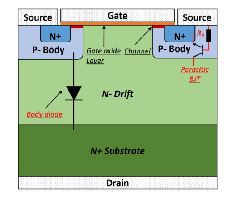
Cross-sectional view of a typical Power MOSFET
Vertical Structure
Unlike regular MOSFETs, power MOSFETs employ a vertical structure where current flows from top (source) to bottom (drain), maximizing current handling capacity.
Drift Region
Contains a lightly doped n- region that supports high blocking voltage and manages electric field distribution.
Key Structural Components
- Source Metal: Top metal layer for current collection and distribution
- n+ Source Regions: Heavily doped regions for carrier injection
- p-Body Region: Creates the channel for current flow
- n- Drift Region: Supports voltage blocking capability
- n+ Substrate: Provides low resistance path to drain
- Drain Metal: Bottom metal contact for current flow
Design Consideration
The cell pitch and junction depth are critical parameters that affect the device’s performance characteristics including on-resistance and switching speed.
Cell Structure Details
Key Dimensional Parameters
- Cell Pitch: Typically 2-10 μm
- Gate Oxide Thickness: 50-100 nm
- Junction Depth: 1-3 μm
- Drift Region Thickness: 5-50 μm (voltage dependent)
Structural Layer Analysis
Gate Structure
┌──────────────┐
│ Gate Oxide │
════╝ SiO2 ╚════
- Polysilicon material for gate electrode
- Optimized gate oxide thickness for reliability
- Specialized gate geometry for uniform field distribution
- Multiple parallel cells for current handling
Channel Formation
    Gate
    ║
 S  ▼  S
═╗ ═══ ╔═
 ║ Chr ║    ← Inversion
n+╚═══╝n+      Channel
   p-body     Formation
    │
    │  n-
    │
Channel formation under gate bias
Advanced Structural Features
Trench Structure
    S   G   S
    ┌─╨─┐
    │   │
n+ ═╣   ╠═ n+
    │   │
    │   │
p   │   │   p
    │   │
    └───┘
     n-
Modern trench design for reduced on-resistance
Planar Structure
    S  G  S
    ╨  ╨  ╨
 ═══╗   ╔═══
n+ ═╝   ╚═ n+
    p     p
      n-
Traditional planar design with proven reliability
Design Evolution
Modern power MOSFETs often incorporate advanced features like:
- Super-junction structures
- Charge-balanced columns
- Shield electrodes
- Advanced termination structures
Current Flow Path
Current Flow Direction
    Source
    ↓ ↓ ↓
    ═══════
n+  ║     ║  n+
    ║  →  ║
p   ║  ↓  ║   p
    ║  ↓  ║
    ║  ↓  ║
     n-
    ║  ↓  ║
    ↓ ↓ ↓
    Drain
Vertical current flow pattern in power MOSFET
Edge Termination Structure
Active Area │ Termination Region
           │
═══════════│════════════════
   Active  │  Guard Rings
    Cells  │    ┌─┐ ┌─┐
═══════════│════╧═╧═╧═╧════
           │
    n-     │     Field Plate
           │
═══════════│════════════════
Edge termination design for voltage blocking
Termination Features
- Field rings for electric field distribution
- Field plates for enhanced blocking voltage
- Junction termination extension (JTE)
- Floating guard rings
Device Parameters and Dimensions
Critical Dimensions
| Parameter | Typical Range |
|---|---|
| Channel Length | 0.5 – 2 μm |
| Cell Pitch | 2 – 10 μm |
| Drift Region | 5 – 50 μm |
| Gate Oxide | 50 – 100 nm |
Manufacturing Considerations
- Precise control of doping profiles
- Optimized thermal budget management
- Critical alignment requirements
- Surface passivation quality


