
Transconductance (gm) is a fundamental parameter in MOSFET operation that defines the relationship between input voltage and output current. As a crucial characteristic for analog circuit design, understanding transconductance helps engineers optimize their designs for better performance and efficiency.
What is MOSFET Transconductance?
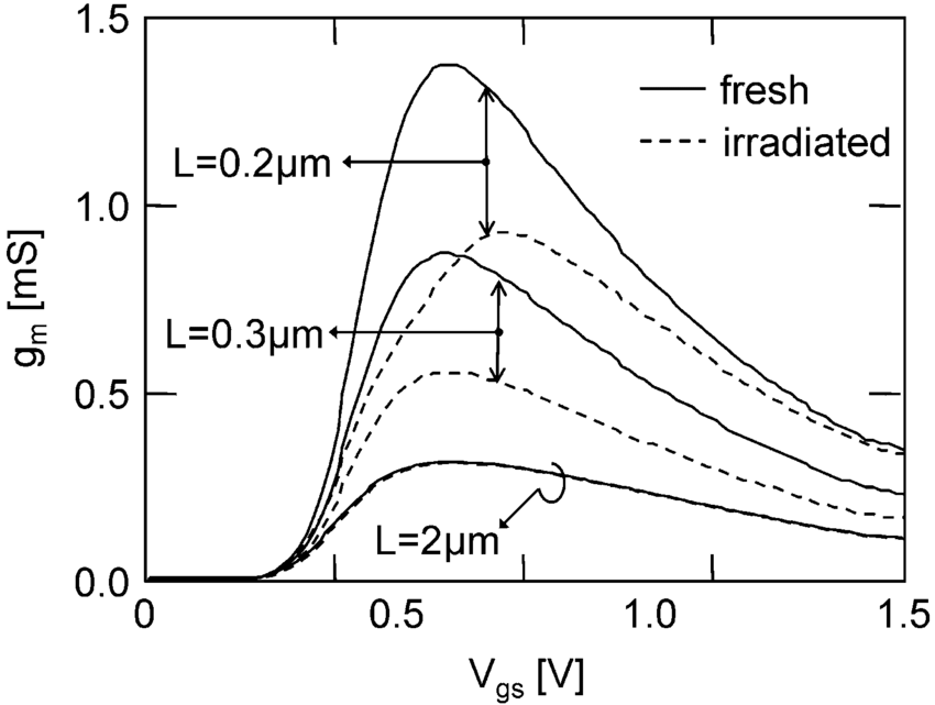 MOSFET transconductance, commonly denoted as gm, represents the change in drain current (ID) relative to a change in gate-to-source voltage (VGS) while maintaining a constant drain-to-source voltage (VDS). It is essentially a measure of the MOSFET’s ability to convert voltage variations into current variations.
Key Aspects of Transconductance
| Parameter | Description | Significance |
|---|---|---|
| Units | Siemens (S) or mho | Represents conductance (1/Ω) |
| Operating Region | Saturation region | Maximum transconductance achieved |
| Temperature Dependence | Inversely proportional | Decreases as temperature increases |
Factors Affecting Transconductance
Several factors influence the transconductance of a MOSFET:
- Device geometry (W/L ratio)
- Operating point (bias conditions)
- Process technology parameters
- Temperature variations
- Supply voltage
Need high-quality MOSFETs with optimized transconductance parameters? As an authorized MOSFET distributor, Olukey offers premium Winsok MOSFETs designed for superior performance in various applications.
Transconductance in Different Operating Regions
The behavior of transconductance varies significantly across different MOSFET operating regions:
| Operating Region | Transconductance Behavior | Mathematical Expression |
|---|---|---|
| Cutoff Region | Approximately zero | gm ≈ 0 |
| Linear Region | Varies with VDS | gm = μnCox(W/L)VDS |
| Saturation Region | Maximum value | gm = μnCox(W/L)(VGS – VTH) |
Applications and Importance in Circuit Design
Analog Circuit Applications
 Transconductance plays a crucial role in various analog circuit applications:
- Amplifier design and gain calculation
- Frequency response optimization
- Bandwidth determination
- Power efficiency considerations
- Temperature compensation circuits
Working on a challenging analog design project? As a leading semiconductor supplier, Olukey provides comprehensive technical support and premium Winsok MOSFETs to meet your specific requirements.
Practical Considerations for Design Engineers
When working with MOSFET transconductance, engineers should consider:
Temperature Effects
Temperature significantly impacts transconductance through:
- Carrier mobility reduction at higher temperatures
- Threshold voltage variation
- Changes in channel resistance
Frequency Considerations
At high frequencies, engineers must account for:
- Parasitic capacitances
- Miller effect
- Transit time limitations
Measurement and Characterization
Measurement Techniques
Accurate transconductance measurement requires:
- Precise voltage and current control
- Temperature stabilization
- Proper biasing conditions
- Advanced measurement equipment
Practical Measurement: gm = ΔID/ΔVGS
(for small signal conditions where ΔVGS is typically 50-100mV)
Common Challenges and Solutions
| Challenge | Impact | Solution |
|---|---|---|
| Temperature Variation | Unstable measurements | Use temperature-controlled test fixtures |
| Noise | Measurement inaccuracy | Implement proper shielding and filtering |
| Device Degradation | Parameter drift | Regular calibration and reference devices |
Future Trends and Developments
 The semiconductor industry continues to evolve, bringing new developments in MOSFET technology:
- Advanced manufacturing processes for higher transconductance
- Novel materials for improved performance
- Better temperature stability
- Enhanced high-frequency operation
Stay ahead of the curve with Olukey’s cutting-edge Winsok MOSFETs. As an authorized electronics distributor, we provide the latest semiconductor solutions backed by expert technical support.
Expert Support and Resources
Understanding and optimizing MOSFET transconductance requires expertise and proper technical support. Olukey provides:
- Comprehensive technical documentation
- Expert application support
- Sample programs for evaluation
- Design consultation services
- Reliable supply chain solutions
Ready to optimize your design with high-performance MOSFETs? Contact Olukey’s technical team for professional support and solutions.
MOSFET Transconductance: Practical Circuit Design Cases
1. Small Signal Amplifier Design
In small signal amplifiers, gm directly determines the voltage gain:
Voltage Gain (Av) = -gm × RD
where RD is the drain resistance
Design Example:
For a common-source amplifier with:
- Required gain: -10 V/V
- Drain resistance: 2.5 kΩ
- Required gm = |10|/2.5k = 4 mA/V
- Operating point: ID = 1mA, VGS = 2.5V
Need MOSFETs optimized for amplifier applications? Olukey offers Winsok’s precision-engineered MOSFETs with excellent transconductance linearity. View our amplifier-grade MOSFETs.
2. RF Front-End Design
In RF applications, gm affects:
- Input impedance matching
- Noise figure optimization
- Power gain
LNA Design Case:
For a 2.4GHz Low Noise Amplifier:
- Required power gain: 15dB
- Noise figure target: < 1.5dB
- Optimal gm: 20mS
- Input matching: gm-boosted common-gate topology
3. Voltage-Controlled Oscillator (VCO)
Critical gm considerations in VCO design:
| Parameter | Requirement | gm Impact |
|---|---|---|
| Oscillation Condition | gm × RL > 1 | Startup reliability |
| Phase Noise | Moderate gm | Noise optimization |
| Power Consumption | Efficient gm/ID | Current efficiency |
4. Current Mirror Applications
Precision current mirrors require matched gm values:
High-Precision Mirror Design:
- Required accuracy: 0.1%
- Temperature range: -40°C to +85°C
- gm matching requirement: < 0.05% difference
- Solution: Matched pair MOSFETs with integrated temperature compensation
5. Power Management Circuits
Applications in switching regulators:
- Error amplifier design
- Current sensing
- Overcurrent protection
Buck Converter Case Study:
For a 12V to 3.3V, 5A buck converter:
- Power MOSFET gm: 25 S
- Error amp gm: 200 μA/V
- Current sense gm: 10 mA/V
- Switching frequency: 500 kHz
Working on power management designs? As a professional MOSFET supplier, Olukey provides comprehensive power MOSFET solutions with detailed application support.
6. Transimpedance Amplifiers (TIA)
Critical specifications for optical receiver TIAs:
| Parameter | Typical Value | gm Requirement |
|---|---|---|
| Bandwidth | 1 GHz | gm > 20 mA/V |
| Input referred noise | < 5 pA/√Hz | Optimized gm/ID |
| Transimpedance gain | 10 kΩ | gm × RF product |
Design Optimization Tips:
- Always consider gm/ID ratio for power efficiency
- Account for temperature effects on gm
- Use matched devices for differential pairs
- Monitor process variations impact on gm
Need assistance with your analog circuit design? Our technical team provides expert guidance on MOSFET selection and application optimization.


-

Why are MOSFETs voltage controlled?
-

Ideas to solve the serious heat generation of M...
-

Do you know about depletion MOSFETs?
-

What are the main features of MOSFETs?
-

Do you know the definition of MOSFET?
-

Analysis of important causes of MOSFET heat gen...
-

MOSFET Solid State Relay Circuits: Revolutionar...
-
Large Package MOSFET Design Knowledge
-

How to determine whether a MOSFET is good or bad?
-

MOSFET Overdrive Voltage: Complete Analysis and...
-

Using a MOSFET as a Switch: Complete Implementa...
-

Causes and Prevention of MOSFET Failure
-

MOSFET Operating Characteristics
-

FET DFN2X2 package single P-channel 20V-40V mod...
-

What Is a Switched Mode Power Supply?
-
What are the functions of MOSFET?


