
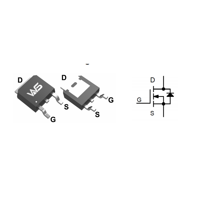
Looking for high-performance MOSFETs for your gain-stacking applications? As an authorized distributor of WINSOK semiconductors, Olukey offers premium-quality MOSFETs with superior gain characteristics and reliability.
The Fundamentals of MOSFET Gain Stacking
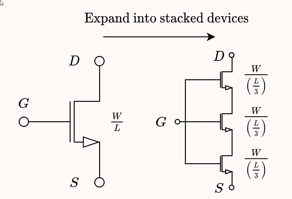
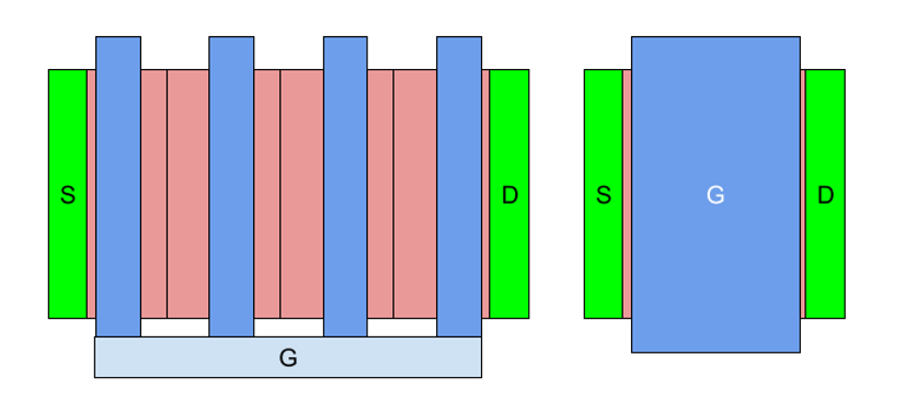 MOSFET stacking has become increasingly important in modern electronic design, particularly when specific gain requirements need to be met. This advanced technique allows engineers to achieve higher voltage handling capabilities and improved gain characteristics that wouldn’t be possible with single devices.
Why Stack MOSFETs?
Before diving into the stacking techniques, it’s crucial to understand the key benefits:
- Increased voltage handling capability
- Enhanced power efficiency
- Improved thermal management
- Better overall system reliability
- Reduced individual component stress
Common Stacking Configurations
| Configuration | Gain Enhancement | Typical Applications |
|---|---|---|
| Series Stacking | 2-3x per stage | High voltage applications |
| Parallel Stacking | 1.5-2x current capability | High current applications |
| Cascode Configuration | 4-5x voltage gain | RF amplifiers |
Explore Our MOSFET Selection →
Technical Implementation Guide
Basic Stacking Calculations
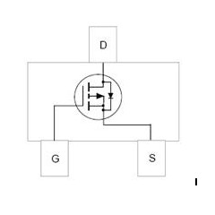
When stacking MOSFETs for gain enhancement, several key parameters must be considered:
Essential Formula:
Total Gain = Gm1 × Gm2 × RL
where Gm1 and Gm2 are the transconductance of each MOSFET, and RL is the load resistance
Total Gain = Gm1 × Gm2 × RL
where Gm1 and Gm2 are the transconductance of each MOSFET, and RL is the load resistance
Step-by-Step Stacking Process
- Select appropriate MOSFETs based on voltage requirements
- Calculate individual MOSFET transconductance
- Determine optimal biasing points
- Implement voltage divider network
- Add necessary protection components

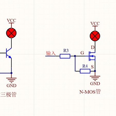
Practical Design Considerations
Need expert guidance on MOSFET selection? Olukey’s technical team offers professional consultation services. As a leading supplier of WINSOK MOSFETs, we ensure optimal component matching for your stacking applications.
Component Selection Guidelines
| Parameter | Recommendation | Critical Considerations |
|---|---|---|
| Voltage Rating | 1.5x required voltage | Safety margin for transients |
| Current Rating | 2x expected current | Thermal management |
| Gate Threshold | Similar Vth values | Matching characteristics |
Common Challenges and Solutions
Key Challenges:
- Voltage balancing between stacked devices
- Temperature management
- Switching synchronization
- Gate drive complexity
Advanced Implementation Tips
 For optimal performance in MOSFET stacking applications, consider these professional recommendations:
- Use matched pairs of MOSFETs when possible
- Implement proper thermal management solutions
- Consider parasitic effects in PCB layout
- Add snubber circuits for switching applications
- Monitor individual MOSFET temperatures
Professional Support from Olukey
As WINSOK’s authorized distributor, we offer:
- Technical consultation for MOSFET stacking applications
- Premium-quality MOSFETs with matched characteristics
- Comprehensive documentation and application support
- Reliable supply chain and competitive pricing
Future Trends and Developments
 The field of MOSFET stacking continues to evolve with new technologies and methodologies:
- Advanced gate drive ICs specifically designed for stacked configurations
- Improved thermal management solutions
- Integration with wide-bandgap semiconductor technologies
- Enhanced protection and monitoring features


-

Detailed explanation of the working principle o...
-
What parameters should I pay attention to when ...
-
What are the differences between MOSFETs and Tr...
-

The three pins of a MOSFET, how can I tell them...
-

High Voltage Gate Drivers: Powering Next-Genera...
-
What is a MOSFET? What are the main parameters?
-

MOSFET Voltage-Controlled Resistor: Advanced Ap...
-

Testing MOSFET Transistors: A Professional̵...
-
MOSFET Package Switching Tube Selection and Cir...
-

Basic Understanding of MOSFET
-

2N2222 Transistor: The Versatile Workhorse of E...
-

TFET vs MOSFET: Understanding the Future of Tra...
-

Enhancement Mode and Depletion Mode MOSFET: A D...
-

How to determine whether a MOSFET is good or bad?
-
What is the role of small voltage MOSFETs?


