


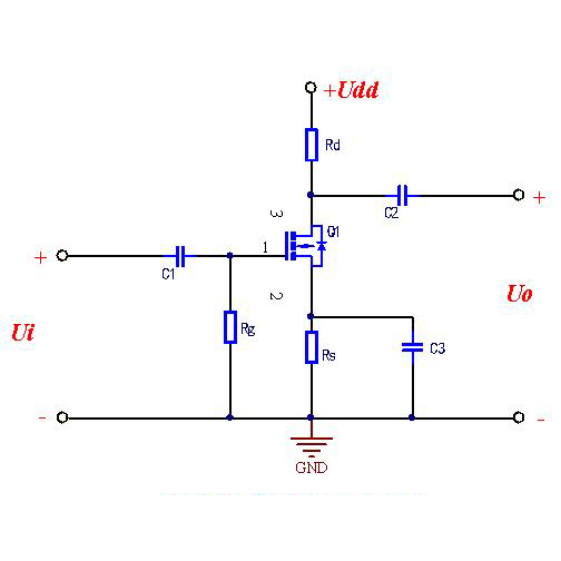
(1) The control effect of vGS on ID and channel
① Case of vGS=0
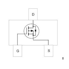
It can be seen that there are two back-to-back PN junctions between the drain d and source s of the enhancement-mode MOSFET.
When the gate-source voltage vGS=0, even if the drain-source voltage vDS is added, and regardless of the polarity of vDS, there is always a PN junction in the reverse biased state. There is no conductive channel between the drain and the source, so the drain current ID≈0 at this time.
② The case of vGS>0
If vGS>0, an electric field is generated in the SiO2 insulating layer between the gate and the substrate. The direction of the electric field is perpendicular to the electric field directed from the gate to the substrate on the semiconductor surface. This electric field repels holes and attracts electrons. Repelling holes: The holes in the P-type substrate near the gate are repelled, leaving immovable acceptor ions (negative ions) to form a depletion layer. Attract electrons: The electrons (minority carriers) in the P-type substrate are attracted to the substrate surface.
(2) Formation of conductive channel:
When the vGS value is small and the ability to attract electrons is not strong, there is still no conductive channel between the drain and the source. As vGS increases, more electrons are attracted to the surface layer of the P substrate. When vGS reaches a certain value, these electrons form an N-type thin layer on the surface of the P substrate near the gate and are connected to the two N+ regions, forming an N-type conductive channel between the drain and source. Its conductivity type is opposite to that of the P substrate, so it is also called an inversion layer. The larger vGS is, the stronger the electric field acting on the semiconductor surface is, the more electrons are attracted to the surface of the P substrate, the thicker the conductive channel is, and the smaller the channel resistance is. The gate-source voltage when the channel begins to form is called the turn-on voltage, represented by VT.
The N-channel MOSFET discussed above cannot form a conductive channel when vGS < VT, and the tube is in a cut-off state. Only when vGS≥VT can a channel be formed. This kind of MOSFET that must form a conductive channel when vGS≥VT is called an enhancement-mode MOSFET. After the channel is formed, a drain current is generated when a forward voltage vDS is applied between the drain and source. The influence of vDS on ID, when vGS>VT and is a certain value, the influence of drain-source voltage vDS on the conductive channel and current ID is similar to that of junction field effect transistor. The voltage drop generated by the drain current ID along the channel makes the voltages between each point in the channel and the gate no longer equal. The voltage at the end close to the source is the largest, where the channel is thickest. The voltage at the drain end is the smallest, and its value is VGD=vGS-vDS, so the channel is the thinnest here. But when vDS is small (vDS<vGS–VT), it has little effect on the channel. At this time, as long as vGS is constant, the channel resistance is almost constant, so ID changes approximately linearly with vDS. As vDS increases, the channel near the drain becomes thinner and thinner. When vDS increases to VGD=vGS-vDS=VT (or vDS=vGS-VT), the channel appears pre-pinched at the drain end. . As vDS continues to increase, the pinch-off point will move toward the source. Since the increase in vDS almost all falls in the pinch-off zone, the ID almost does not increase with the increase in vDS. The tube enters the saturation zone, and the ID is almost only determined by vGS.
-
The three main roles of MOSFETs
-

Basic Requirements for MOSFET Driver Circuits
-

How to determine whether a MOSFET is good or bad?
-
Characteristics of MOSFETs and Precautions for Use
-
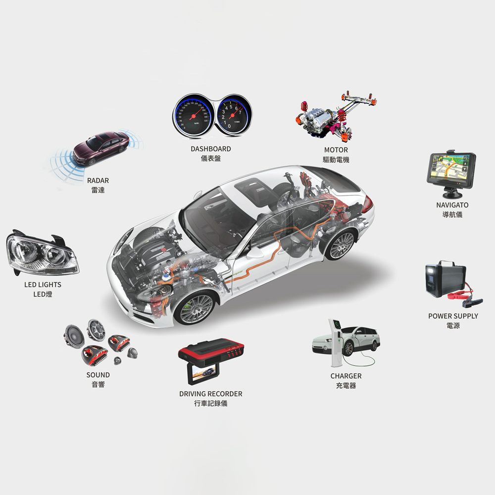
What are the application scenarios for MOSFETs?
-

Characteristics of Enhanced MOSFETs
-
MOSFET Package Switching Tube Selection and Cir...
-

Olukey: Let’s talk about the role of MOSFET in ...
-

The connection between MOSFETs and Field Effect...
-
Why is it always difficult to test high power M...
-

Gate capacitance, on-resistance and other param...
-

Parameter analysis and measurement of MOSFETs
-
How Enhanced Package MOSFETs Work
-
What are the functions of MOSFET?
-

A Comprehensive Guide: How to Add and Simulate ...
-

Do you know the definition of MOSFET?


