


There are many varieties of MOSFETs, mainly divided into junction MOSFETs and insulated gate MOSFETs two categories, and all have N-channel and P-channel points.
Metal-Oxide-Semiconductor Field-Effect Transistor, referred to as MOSFET, is divided into depletion type MOSFET and enhancement type MOSFET.
MOSFETs are also divided into single-gate and dual-gate tubes. Dual-gate MOSFET has two independent gate G1 and G2, from the construction of the equivalent of two single-gate MOSFETs connected in series, and its output current changes by the two gate voltage control. This characteristic of dual-gate MOSFETs brings great convenience when used as high-frequency amplifiers, gain control amplifiers, mixers and demodulators.
1, MOSFET type and structure
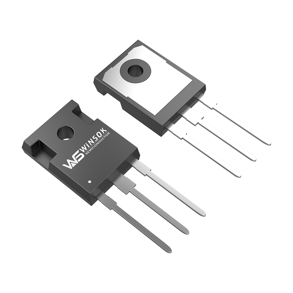
MOSFET is a kind of FET (another kind is JFET), can be manufactured into enhanced or depletion type, P-channel or N-channel a total of four types, but the theoretical application of only enhanced N-channel MOSFET and enhanced P-channel MOSFET, so usually referred to as NMOS, or PMOS refers to these two kinds. As for why not use depletion type MOSFETs, do not recommend the search for the root cause. Regarding the two enhanced MOSFETs, the more commonly used is NMOS, the reason is that the on-resistance is small, and easy to manufacture. So switching power supply and motor drive applications, generally use NMOS. the following quote, but also more NMOS-based. three pins of the MOSFET parasitic capacitance exists between the three pins, which is not our needs, but due to manufacturing process limitations. The existence of parasitic capacitance in the design or selection of the drive circuit to save some time, but there is no way to avoid, and then detailed introduction. In the MOSFET schematic diagram can be seen, the drain and source between a parasitic diode. This is called the body diode, in driving rational loads, this diode is very important. By the way, the body diode only exists in a single MOSFET, usually not inside the integrated circuit chip.
2, MOSFET conduction characteristics
The significance of conduction is as a switch, equivalent to a switch closure.NMOS characteristics, Vgs greater than a certain value will conduct, suitable for use in the case when the source is grounded (low-end drive), only the gate voltage arrives at 4V or 10V.PMOS characteristics, Vgs less than a certain value will conduct, suitable for use in the case when the source is connected to the VCC (high-end drive).
However, of course, PMOS can be very easy to use as a high-end driver, but due to the on-resistance, expensive, less types of exchanges and other reasons, in the high-end driver, usually still use NMOS.
3, MOSFET switching loss
Whether it is NMOS or PMOS, after the on-resistance exists, so that the current will consume energy in this resistance, this part of the energy consumed is called the on-resistance loss. Selecting a MOSFET with a small on-resistance will reduce the on-resistance loss. The usual low-power MOSFET on-resistance is usually in the tens of milliohms, a few milliohms there. MOS in the on-time and cut-off, must not be in the instantaneous completion of the voltage across the MOS there is a process of falling, the current flowing through a process of rising, during this time, the loss of the MOSFET is the product of the voltage and current is called the switching loss. Usually the switching loss is much larger than the conduction loss, and the faster the switching frequency, the larger the loss. A large product of voltage and current at the instant of conduction constitutes a large loss. Shortening the switching time reduces the loss at each conduction; reducing the switching frequency reduces the number of switches per unit time. Both approaches can reduce the switching loss.
4, MOSFET drive
Compared to bipolar transistors, it is commonly assumed that no current is required to make the MOSFET conduct, only that the GS voltage is above a certain value. This is easy to do, however, we also need speed. In the structure of the MOSFET you can see that there is a parasitic capacitance between GS, GD, and the driving of the MOSFET is, in theory, the charging and discharging of the capacitance. Charging the capacitor requires a current, and since charging the capacitor instantly can be viewed as a short circuit, the instantaneous current will be high. Selection / design of MOSFET drive the first thing to pay attention to is the size of the instantaneous short-circuit current can be provided. The second thing to pay attention to is that, generally used in high-end drive NMOS, on demand is the gate voltage is greater than the source voltage. High-end drive MOS tube conduction source voltage and drain voltage (VCC) the same, so the gate voltage than the VCC 4V or 10V. assuming that in the same system, to get a larger voltage than the VCC, we need a special boost circuit. Many motor drivers are integrated charge pump, to pay attention to is should choose the appropriate external capacitor, in order to get enough short-circuit current to drive the MOSFET. 4V or 10V said above is commonly used MOSFET on voltage, the design of course, the need to have a certain margin. The higher the voltage, the faster the on-state speed and the lower the on-state resistance. Usually there are also smaller on-state voltage MOSFETs used in different categories, but in 12V automotive electronics systems, ordinary 4V on-state is enough.
The main parameters of the MOSFET are as follows:
1. gate source breakdown voltage BVGS - in the process of increasing the gate source voltage, so that the gate current IG from zero to start a sharp increase in VGS, known as the gate source breakdown voltage BVGS.
2. turn-on voltage VT - turn-on voltage (also known as the threshold voltage): make the source S and drain D between the beginning of the conductive channel constitutes the gate voltage required; - standardized N-channel MOSFET, VT is about 3 ~ 6V; - after the process of improvement, can make the MOSFET VT value down to 2 ~ 3V.
3. Drain breakdown voltage BVDS - under the condition of VGS = 0 (reinforced) , in the process of increasing the drain voltage so that the ID starts to increase dramatically when the VDS is called the drain breakdown voltage BVDS - ID dramatically increased due to the following two aspects:
(1) avalanche breakdown of the depletion layer near the drain electrode
(2) drain-source inter-pole penetration breakdown - some small voltage MOSFET, its channel length is short, from time to time to increase the VDS will make the drain region of the depletion layer from time to time to expand to the source region, so that the channel length of zero, that is, between the drain-source penetration, penetration, the source region of the majority of carriers, the source region, will be straight to withstand the depletion layer of the absorption of the electric field, to arrive at the leakage region, resulting in a large ID.
4. DC input resistance RGS-i.e., the ratio of the voltage added between the gate source and the gate current, this characteristic is sometimes expressed in terms of the gate current flowing through the gate MOSFET's RGS can easily exceed 1010Ω. 5.
5. low-frequency transconductance gm in the VDS for a fixed value of the conditions, the microvariance of the drain current and the gate source voltage microvariance caused by this change is called the transconductance gm, reflecting the control of the gate source voltage on the drain current is to show that the MOSFET amplification of an important parameter, generally in the range of a few to a few mA / V. The MOSFET can easily exceed 1010Ω.
-
How Enhanced Package MOSFETs Work
-
MOSFET Selection Points
-

The difference between N-channel MOSFET and P-c...
-
The connection between MOSFETs and Field Effect...
-

The role of MOSFETs in circuits
-
What are the four regions of a MOSFET?
-

Do You Know About MOSFET Circuits?
-

The Ultimate Guide to Electronic Component Data...
-
MOSFET small current heating causes and measures
-

Causes and Prevention of MOSFET Failure
-

Take a look at MOSFETs
-

What is MOSFET?
-
What are the uses of MOSFETs?
-

De rol van vermogens-MOSFET-apparaten
-

How to prevent MOSFET failure
-
How to choose a MOSFET?


