


The same high-power MOSFET, the use of different drive circuits will get different switching characteristics. The use of good performance of the drive circuit can make the power switching device work in a relatively ideal switching state, while shortening the switching time, reduce switching losses, the installation of the operating efficiency, reliability and safety are of great significance. Therefore, the advantages and disadvantages of the drive circuit directly affects the performance of the main circuit, the rationalization of the design of the drive circuit is increasingly important. Thyristor small size, light weight, high efficiency, long life, easy to use, can easily stop the rectifier and inverter, and can not change the circuit structure under the premise of changing the size of the rectifier or inverter current.IGBT is a composite device of MOSFET and GTR, which has the characteristics of fast switching speed, good thermal stability, small driving power and simple drive circuit, and has the advantages of small on-state voltage drop, high withstand voltage and high acceptance current. IGBT as a mainstream power output device, especially in high-power places, has been commonly used in various categories.
The ideal driving circuit for high-power MOSFET switching devices should meet the following requirements:
(1) When the power switching tube is turned on, the driving circuit can provide a fast-rising base current, so that there is enough driving power when it is turned on, thus reducing the turn-on loss.
(2) During the switching tube conduction, the base current provided by the MOSFET driver circuit can ensure that the power tube is in saturated conduction state under any load condition, ensuring comparatively low conduction loss. In order to reduce the storage time, the device should be in a critical saturation state before shutdown.
(3) shutdown, the drive circuit should provide sufficient reverse base drive to quickly draw out the remaining carriers in the base region to reduce the storage time; and add reverse bias cutoff voltage, so that the collector current falls rapidly to reduce the landing time. Of course, the shutdown of the thyristor is still mainly by the reverse anode voltage drop to complete the shutdown.
At present, the thyristor drive with a comparable number of just through the transformer or optocoupler isolation to separate the low voltage end and high voltage end, and then through the conversion circuit to drive the thyristor conduction. On the IGBT for the current use of more IGBT drive module, but also integrated IGBT, system self-maintenance, self-diagnosis and other functional modules of the IPM.
In this paper, for the thyristor we use, design experimental drive circuit, and stop the real test to prove that it can drive the thyristor. As for the drive of IGBT, this paper mainly introduces the current main types of IGBT drive, as well as their corresponding drive circuit, and the most commonly used optocoupler isolation drive to stop the simulation experiment.
2. Thyristor drive circuit study in general the thyristor operating conditions are:
(1) the thyristor accepts the reverse anode voltage, regardless of the gate accepts what kind of voltage, the thyristor is in the off state.
(2) Thyristor accepts forward anode voltage, only in the case of the gate accepts a positive voltage the thyristor is on.
(3) Thyristor in the conduction condition, only a certain positive anode voltage, regardless of the gate voltage, the thyristor insisted on conduction, that is, after the thyristor conduction, the gate is lost. (4) thyristor in the conduction condition, when the main circuit voltage (or current) reduced to near zero, the thyristor shutdown. We choose the thyristor is TYN1025, its withstand voltage is 600V to 1000V, current up to 25A. it requires the gate drive voltage is 10V to 20V, drive current is 4mA to 40mA. and its maintenance current is 50mA, the engine current is 90mA. either DSP or CPLD trigger signal amplitude as long as 5V. First of all, as long as the amplitude of 5V into 24V, and then through a 2:1 isolation transformer to convert the 24V trigger signal into a 12V trigger signal, while completing the function of the upper and lower voltage isolation.
Experimental circuit design and analysis
First of all, the boost circuit, due to the isolation transformer circuit in the back stage of the MOSFET device needs 15V trigger signal, so the need to first amplitude 5V trigger signal into a 15V trigger signal, through the MC14504 5V signal, converted into a 15V signal, and then through the CD4050 on the output of the 15V drive signal shaping, channel 2 is connected to the 5V input signal, channel 1 is connected to the output Channel 2 is connected to the 5V input signal, channel 1 is connected to the output of the 15V trigger signal.
The second part is the isolation transformer circuit, the main function of the circuit is: the 15V trigger signal, converted into a 12V trigger signal to trigger the back of the thyristor conduction, and to do the 15V trigger signal and the distance between the back stage.
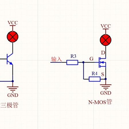
The working principle of the circuit is: due to the MOSFET IRF640 drive voltage of 15V, so, first of all, in J1 access to 15V square wave signal, through the resistor R4 connected to the regulator 1N4746, so that the trigger voltage is stable, but also to make the trigger voltage is not too high, burned MOSFET, and then to the MOSFET IRF640 (in fact, this is a switching tube, the control of the back end of the opening and closing. Control the back end of the turn-on and turn-off), after controlling the duty cycle of the drive signal, to be able to control the turn-on and turn-off time of the MOSFET. When the MOSFET is open, equivalent to its D-pole ground, off when it is open, after the back-end circuit equivalent to 24 V. And the transformer is through the voltage change to make the right end of the 12 V output signal. The right end of the transformer is connected to a rectifier bridge, and then the 12V signal is output from connector X1.
Problems encountered during the experiment
First of all, when the power was turned on, the fuse suddenly blew, and later when checking the circuit, it was found that there was a problem with the initial circuit design. Initially, in order to better the effect of its switching tube output, the 24V ground and 15V ground separation, which makes the MOSFET's gate G pole equivalent to the back of the S pole is suspended, resulting in false triggering. Treatment is to connect the 24V and 15V ground together, and again to stop the experiment, the circuit works normally. Circuit connection is normal, but when participating in the drive signal, MOSFET heat, plus drive signal for a period of time, the fuse is blown, and then add the drive signal, the fuse is directly blown. Check the circuit found that the high level duty cycle of the drive signal is too large, resulting in the MOSFET turn-on time is too long. The design of this circuit makes when the MOSFET open, 24V added directly to the ends of the MOSFET, and did not add a current-limiting resistor, if the on-time is too long to make the current is too large, MOSFET damage, the need to regulate the duty cycle of the signal can not be too large, generally in the 10% to 20% or so.
2.3 Verification of the drive circuit
In order to verify the feasibility of the drive circuit, we use it to drive the thyristor circuit connected in series with each other, the thyristor in series with each other and then anti-parallel, access to the circuit with inductive reactance, the power supply is 380V AC voltage source.
MOSFET in this circuit, the thyristor Q2, Q8 trigger signal through the G11 and G12 access, while Q5, Q11 trigger signal through the G21, G22 access. Before the drive signal is received to the thyristor gate level, in order to improve the anti-interference ability of the thyristor, the gate of the thyristor is connected to a resistor and capacitor. This circuit is connected to the inductor and then put into the main circuit. After controlling the conduction angle of the thyristor to control the large inductor into the main circuit time, the upper and lower circuits of the phase angle of the trigger signal difference of half a cycle, the upper G11 and G12 is a trigger signal all the way through the drive circuit of the front stage of the isolation transformer is isolated from each other, the lower G21 and G22 is also isolated from the same way the signal. The two trigger signals trigger anti-parallel thyristor circuit positive and negative conduction, above the 1 channel is connected to the entire thyristor circuit voltage, in the thyristor conduction it becomes 0, and 2, 3 channel is connected to the thyristor circuit up and down the road trigger signals, the 4 channel is measured by the flow of the entire thyristor current.
2 channel measured a positive trigger signal, triggered above the thyristor conduction, the current is positive; 3 channel measured a reverse trigger signal, triggering the lower circuit of the thyristor conduction, the current is negative.
3.IGBT drive circuit of the seminar IGBT drive circuit has many special requests, summarized:
(1) drive the rate of rise and fall of the voltage pulse should be sufficiently large. igbt turn on, the leading edge of the steep gate voltage is added to the gate G and emitter E between the gate, so that it is quickly turned on to reach the shortest turn on time to reduce turn on losses. In the IGBT shutdown, the gate drive circuit should provide the IGBT landing edge is very steep shutdown voltage, and to the IGBT gate G and emitter E between the appropriate reverse bias voltage, so that the IGBT fast shutdown, shorten the shutdown time, reduce the shutdown loss.
(2) After IGBT conduction, the drive voltage and current provided by the gate drive circuit should be sufficient amplitude for the IGBT drive voltage and current, so that the power output of the IGBT is always in a saturated state. Transient overload, the driving power provided by the gate drive circuit should be sufficient to ensure that the IGBT does not exit the saturation region and damage.
(3) IGBT gate drive circuit should provide IGBT positive drive voltage to take the appropriate value, especially in the short-circuit operating process of the equipment used in the IGBT, the positive drive voltage should be selected to the minimum value required. Switching application of the gate voltage of the IGBT should be 10V ~ 15V for the best.
(4) IGBT shutdown process, the negative bias voltage applied between the gate - emitter is conducive to the rapid shutdown of the IGBT, but should not be taken too large, ordinary take -2V to -10V.
(5) in the case of large inductive loads, too fast switching is harmful, large inductive loads in the IGBT rapid turn-on and turn-off, will produce high-frequency and high amplitude and narrow width of the spike voltage Ldi / dt, the spike is not easy to absorb, easy to form device damage.
(6) As the IGBT is used in high-voltage places, so the drive circuit should be with the entire control circuit in the potential of severe isolation, the ordinary use of high-speed optical coupling isolation or transformer coupling isolation.
Drive circuit status
With the development of integrated technology, the current IGBT gate drive circuit is mostly controlled by integrated chips. The control mode is still mainly three kinds:
(1) direct triggering type no electrical isolation between the input and output signals.
(2) transformer isolation drive between the input and output signals using pulse transformer isolation, isolation voltage level up to 4000V.
There are 3 approaches as follows
Passive approach: the output of the secondary transformer is used to directly drive the IGBT, due to the limitations of the volt-second equalization, it is only applicable to places where the duty cycle does not change much.
Active method: the transformer only provides isolated signals, in the secondary plastic amplifier circuit to drive IGBT, drive waveform is better, but the need to provide separate auxiliary power.
Self-supply method: pulse transformer is used to transmit both drive energy and high-frequency modulation and demodulation technology for transmission of logic signals, divided into modulation-type self-supply approach and time-sharing technology self-supply, in which the modulation-type self-supply power to the rectifier bridge to generate the required power supply, high-frequency modulation and demodulation technology to transmit logic signals.
3. Contact and difference between thyristor and IGBT drive
Thyristor and IGBT drive circuit has a difference between the similar center. First of all, the two drive circuits are required to isolate the switching device and the control circuit from each other, so as to avoid high-voltage circuits have an impact on the control circuit. Then, both are applied to the gate drive signal to trigger the switching device on. The difference is that the thyristor drive requires a current signal, while the IGBT requires a voltage signal. After the switching device conduction, the gate of the thyristor has lost control of the use of the thyristor, if you want to shut down the thyristor, the thyristor terminals should be added to the reverse voltage; and IGBT shutdown only need to be added to the gate of the negative driving voltage, to shut down the IGBT.
4. Conclusion
This paper is mainly divided into two parts of the narrative, the first part of the thyristor drive circuit request to stop the narrative, the design of the corresponding drive circuit, and the design of the circuit is applied to the practical thyristor circuit, through simulation and experimentation to prove the feasibility of the drive circuit, the experimental process encountered in the analysis of the problems stopped and dealt with. The second part of the main discussion on the IGBT on the request of the drive circuit, and on this basis to further introduce the current commonly used IGBT drive circuit, and the main optocoupler isolation drive circuit to stop the simulation and experiment, to prove the feasibility of the drive circuit.
-

MOSFET overview
-

MOSFET substitution principle and good and bad ...
-
What are the differences between MOSFETs and Tr...
-

Why are N channel MOSFET preferred over P chann...
-

Understanding the 4407A MOSFET: Your Friendly G...
-

Do you know what an N-channel MOSFET is?
-

Original spot CMS79F726 package SOP20 touch but...
-

How to determine the high-power MOSFET is burne...
-

Take a look at MOSFETs
-

Understanding the function and structure of MOS...
-
About the working principle of power MOSFET
-

Is the MOSFET fully or half controlled?
-

MOSFET Operating Characteristics
-

How much do you know about the MOSFET symbol?
-

MOSFET gate source protection
-

Semiconductor Market Status of Electronic Infor...


