
The metal-oxide-semiconductor field-effect transistor (MOSFET, MOS-FET, or MOS FET) is a type of field-effect transistor (FET), most commonly fabricated by the controlled oxidation of silicon. It has an insulated gate, the voltage of which determines the conductivity of the device.
Its main feature is that there is a silicon dioxide insulating layer between the metal gate and the channel, so it has a high input resistance (up to 1015Ω). It is also divided into N-channel tube and P-channel tube. Usually the substrate (substrate) and the source S are connected together.
According to different conduction modes, MOSFETs are divided into enhancement type and depletion type.
The so-called enhancement type means: when VGS=0, the tube is in a cut-off state. After adding the correct VGS, most carriers are attracted to the gate, thus "enhancing" the carriers in this area and forming a conductive channel. .
The depletion mode means that when VGS=0, a channel is formed. When the correct VGS is added, most carriers can flow out of the channel, thus "depleting" the carriers and turning the tube off.
Distinguish the reason: JFET's input resistance is more than 100MΩ, and the transconductance is very high, when the gate is led, the indoor space magnetic field is very easy to detect the working voltage data signal on the gate, so that the pipeline tends to be up to, or tends to be on-off. If the body induction voltage is immediately added to the gate, because the key electromagnetic interference is strong, the above situation will be more significant. If the meter needle deflects sharply to the left, it means that the pipeline tends to be up to, the drain-source resistor RDS expands, and the amount of drain-source current decreases IDS. Conversely, the meter needle deflects sharply to the right, indicating that the pipeline tends to be on-off, RDS goes down, and IDS goes up. However, the exact direction in which the meter needle is deflected should depend on the positive and negative poles of the induced voltage (positive direction working voltage or reverse direction working voltage) and the working midpoint of the pipeline.
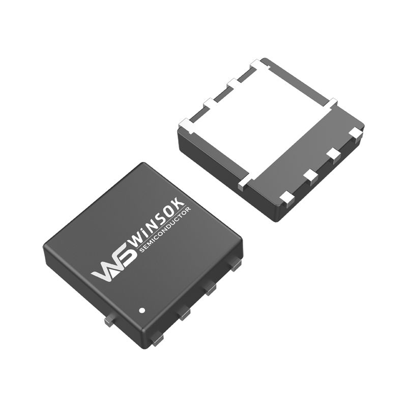
WINSOK DFN3x3 MOSFET
Taking the N channel as an example, it is made on a P-type silicon substrate with two highly doped source diffusion regions N+ and drain diffusion regions N+, and then the source electrode S and the drain electrode D are led out respectively. The source and substrate are internally connected, and they always maintain the same potential. When the drain is connected to the positive terminal of the power supply and the source is connected to the negative terminal of the power supply and VGS=0, the channel current (i.e. drain current) ID=0. As VGS gradually increases, attracted by the positive gate voltage, negatively charged minority carriers are induced between the two diffusion regions, forming an N-type channel from drain to source. When VGS is greater than the turn-on voltage VTN of the tube (generally about +2V), the N-channel tube begins to conduct, forming a drain current ID.
VMOSFET (VMOSFET), its full name is V-groove MOSFET. It is a newly developed high-efficiency, power switching device after MOSFET. It not only inherits the high input impedance of MOSFET (≥108W), but also the small driving current (about 0.1μA). It also has excellent characteristics such as high withstand voltage (up to 1200V), large operating current (1.5A ~ 100A), high output power (1 ~ 250W), good transconductance linearity, and fast switching speed. Precisely because it combines the advantages of vacuum tubes and power transistors, it is being widely used in voltage amplifiers (voltage amplification can reach thousands of times), power amplifiers, switching power supplies and inverters.
As we all know, the gate, source and drain of a traditional MOSFET are roughly on the same horizontal plane on the chip, and its operating current basically flows in the horizontal direction. The VMOS tube is different. It has two major structural features: first, the metal gate adopts a V-shaped groove structure; second, it has vertical conductivity. Since the drain is drawn from the back of the chip, the ID does not flow horizontally along the chip, but starts from the heavily doped N+ region (source S) and flows into the lightly doped N-drift region through the P channel. Finally, it reaches vertically downward to drain D. Because the flow cross-sectional area increases, large currents can pass through. Since there is a silicon dioxide insulating layer between the gate and the chip, it is still an insulated gate MOSFET.
Advantages of use:
MOSFET is a voltage controlled element, while transistor is a current controlled element.
MOSFETs should be used when only a small amount of current is allowed to be drawn from the signal source; transistors should be used when the signal voltage is low and more current is allowed to be drawn from the signal source. MOSFET uses majority carriers to conduct electricity, so it is called a unipolar device, while transistors use both majority carriers and minority carriers to conduct electricity, so it is called a bipolar device.
The source and drain of some MOSFETs can be used interchangeably, and the gate voltage can be positive or negative, making them more flexible than triodes.
MOSFET can operate under very small current and very low voltage conditions, and its manufacturing process can easily integrate many MOSFETs on a silicon chip. Therefore, MOSFET has been widely used in large-scale integrated circuits.
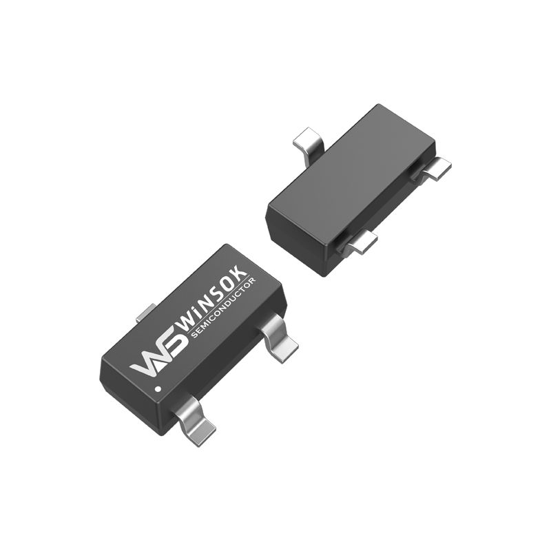
Olueky SOT-23N MOSFET
The respective application characteristics of MOSFET and transistor
1. The source s, gate g, and drain d of the MOSFET correspond to the emitter e, base b, and collector c of the transistor respectively. Their functions are similar.
2. MOSFET is a voltage-controlled current device, iD is controlled by vGS, and its amplification coefficient gm is generally small, so the amplification capability of MOSFET is poor; the transistor is a current-controlled current device, and iC is controlled by iB (or iE).
3. The MOSFET gate draws almost no current (ig»0); while the base of the transistor always draws a certain current when the transistor is working. Therefore, the gate input resistance of the MOSFET is higher than the input resistance of the transistor.
4. MOSFET is composed of multicarriers involved in conduction; transistors have two carriers, multicarriers and minority carriers, involved in conduction. The concentration of minority carriers is greatly affected by factors such as temperature and radiation. Therefore, MOSFETs have better temperature stability and stronger radiation resistance than transistors. MOSFETs should be used where environmental conditions (temperature, etc.) vary greatly.
5. When the source metal and the substrate of MOSFET are connected together, the source and drain can be used interchangeably, and the characteristics change little; while when the collector and emitter of the triode are used interchangeably, the characteristics are very different. The β value will be reduced a lot.
6. The noise coefficient of MOSFET is very small. MOSFET should be used as much as possible in the input stage of low-noise amplifier circuits and circuits that require a high signal-to-noise ratio.
7. Both MOSFET and transistor can form various amplifier circuits and switching circuits, but the former has a simple manufacturing process and has the advantages of low power consumption, good thermal stability, and wide operating power supply voltage range. Therefore, it is widely used in large-scale and very large-scale integrated circuits.
8. The transistor has a large on-resistance, while the MOSFET has a small on-resistance, only a few hundred mΩ. In current electrical devices, MOSFETs are generally used as switches, and their efficiency is relatively high.
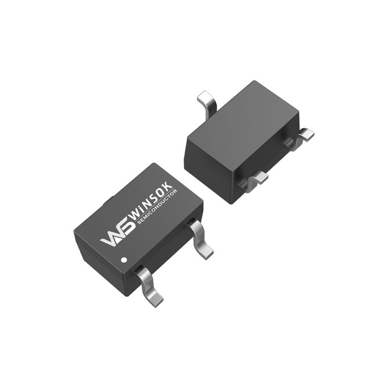
WINSOK SOT-323 encapsulation MOSFET
MOSFET vs. Bipolar Transistor
MOSFET is a voltage-controlled device, and the gate takes basically no current, while a transistor is a current-controlled device, and the base must take a certain current. Therefore, when the rated current of the signal source is extremely small, MOSFET should be used.
MOSFET is a multi-carrier conductor, while both carriers of a transistor participate in conduction. Since the concentration of minority carriers is very sensitive to external conditions such as temperature and radiation, MOSFET is more suitable for situations where the environment changes greatly.
In addition to being used as amplifier devices and controllable switches like transistors, MOSFETs can also be used as voltage-controlled variable linear resistors.
The source and drain of MOSFET are symmetrical in structure and can be used interchangeably. The gate-source voltage of depletion mode MOSFET can be positive or negative. Therefore, using MOSFETs is more flexible than transistors.


-

Take a look at MOSFETs
-

Important Steps on MOSFET Selection
-
Introduction to the working principle of common...
-

Important Steps on MOSFET Selection
-

MOSFET Solid State Relay Circuits: Revolutionar...
-
Difference between output power MOSFET and bipo...
-
Large Package MOSFET Driver Circuit
-

Comprehensive Guide: How to Wire a MOSFET ̵...
-

Mastering MOSFET as a Switch: Complete Implemen...
-

The relationship between MOSFET packaging and p...
-

Characteristics of Enhanced MOSFETs
-

TFET vs MOSFET: Understanding the Future of Tra...
-

Why are MOSFETs voltage controlled?
-

Flow of MOSFET testing
-

D-MOSFET Construction and Working Mechanism: Po...
-

MOSFET Motor Control: Advanced Solutions for Mo...


