When designing a switching power supply or motor drive circuit using MOSFETs, factors such as the on-resistance, maximum voltage, and maximum current of the MOS are generally considered.
MOSFET tubes are a type of FET that can be fabricated as either enhancement or depletion type, P-channel or N-channel for a total of 4 types. enhancement NMOSFETs and enhancement PMOSFETs are generally used, and these two are usually mentioned.
These two are more commonly used is NMOS. the reason is that the conductive resistance is small and easy to manufacture. Therefore, NMOS is usually used in switching power supply and motor drive applications.
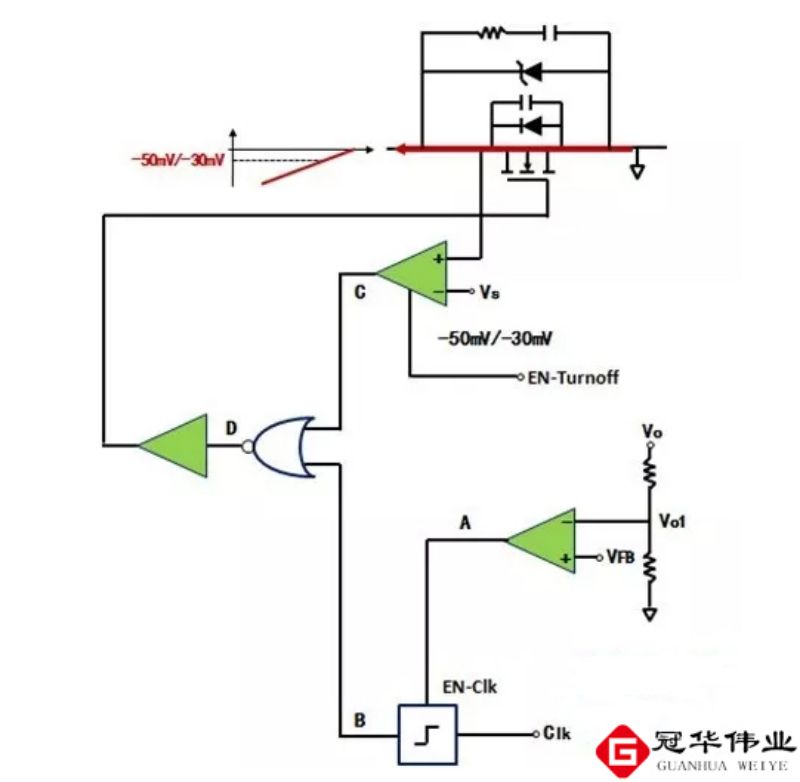
Inside the MOSFET, a thyristor is placed between the drain and the source, which is very important in driving inductive loads such as motors, and is only present in a single MOSFET, not usually in an integrated circuit chip.
Parasitic capacitance exists between the three pins of the MOSFET, not that we need it, but due to limitations of the manufacturing process. The presence of parasitic capacitance makes it more cumbersome when designing or selecting a driver circuit, but it cannot be avoided.
The main parameters of MOSFET
1, open voltage VT
Open voltage (also known as the threshold voltage): so that the gate voltage required to start forming a conductive channel between the source S and drain D; standard N-channel MOSFET, VT is about 3 ~ 6V; through process improvements, the MOSFET VT value can be reduced to 2 ~ 3V.
2, DC input resistance RGS
The ratio of the voltage added between the gate source pole and the gate current This characteristic is sometimes expressed by the gate current flowing through the gate, the MOSFET's RGS can easily exceed 1010Ω.
3. Drain source breakdown BVDS voltage.
Under the condition of VGS = 0 (enhanced), in the process of increasing the drain-source voltage, ID increases sharply when the VDS is called the drain-source breakdown voltage BVDS, ID increases sharply due to two reasons: (1) avalanche breakdown of the depletion layer near the drain, (2) penetration breakdown between the drain and source poles, some MOSFETs, which have a shorter trench length, increase the VDS so that the drain layer in the drain region is expanded to the source region, making the Channel length is zero, that is, to produce a drain-source penetration, penetration, most of the carriers in the source region will be directly attracted by the electric field of the depletion layer to the drain region, resulting in a large ID.
4, gate source breakdown voltage BVGS
When the gate voltage is increased, the VGS when the IG is increased from zero is called the gate source breakdown voltage BVGS.
5、Low frequency transconductance
When VDS is a fixed value, the ratio of the microvariation of the drain current to the microvariation of the gate source voltage that causes the change is called transconductance, which reflects the ability of the gate source voltage to control the drain current, and is an important parameter that characterizes the amplification capability of the MOSFET.
6, on-resistance RON
On-resistance RON shows the effect of VDS on ID, is the inverse of the slope of the tangent line of the drain characteristics at a certain point, in the saturation region, ID almost does not change with the VDS, RON is a very large value, generally in the tens of kilo-Ohms to hundreds of kilo-Ohms, because in digital circuits, MOSFETs often work in the state of the conductive VDS = 0, so at this point, the on-resistance RON can be approximated by the origin of the RON to approximate, for general MOSFET, RON value within a few hundred ohms.
7, inter-polar capacitance
Interpolar capacitance exists between the three electrodes: gate source capacitance CGS, gate drain capacitance CGD and drain source capacitance CDS-CGS and CGD is about 1~3pF, CDS is about 0.1~1pF.
8、Low frequency noise factor
Noise is caused by irregularities in the movement of carriers in the pipeline. Because of its presence, irregular voltage or current variations occur at the output even if there is no signal delivered by the amplifier. Noise performance is usually expressed in terms of the noise factor NF. The unit is decibel (dB). The smaller the value, the less noise the tube produces. The low-frequency noise factor is the noise factor measured in the low-frequency range. The noise factor of a field effect tube is about a few dB, less than that of a bipolar triode.


