


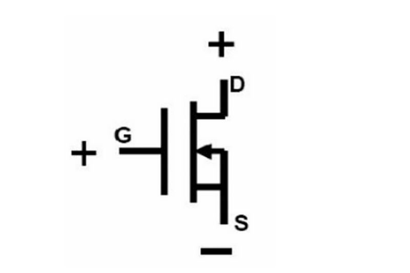
This is a packaged MOSFET pyroelectric infrared sensor. The rectangular frame is the sensing window. The G pin is the ground terminal, the D pin is the internal MOSFET drain, and the S pin is the internal MOSFET source. In the circuit, G is connected to ground, D is connected to the positive power supply, infrared signals are input from the window, and electrical signals are output from S.
Judgment gate G
The MOS driver mainly plays the role of waveform shaping and driving enhancement: If the G signal waveform of the MOSFET is not steep enough, it will cause a large amount of power loss during the switching stage. Its side effect is to reduce the circuit conversion efficiency. The MOSFET will have severe fever and be easily damaged by heat. There is a certain capacitance between MOSFETGS. , if the G signal driving capability is insufficient, it will seriously affect the waveform jump time.
Short-circuit the G-S pole, select the R×1 level of the multimeter, connect the black test lead to the S pole, and the red test lead to the D pole. The resistance should be a few Ω to more than ten Ω. If it is found that the resistance of a certain pin and its two pins are infinite, and it is still infinite after exchanging the test leads, it is confirmed that this pin is the G pole, because it is insulated from the other two pins.
Determine the source S and drain D
Set the multimeter to R×1k and measure the resistance between the three pins respectively. Use the exchange test lead method to measure the resistance twice. The one with a lower resistance value (generally a few thousand Ω to more than ten thousand Ω) is the forward resistance. At this time, the black test lead is the S pole and the red test lead is connected to the D pole. Because of different test conditions, the measured RDS(on) value is higher than the typical value given in the manual.
About MOSFET
The transistor has N-type channel so it is called N-channel MOSFET, or NMOS. P-channel MOS (PMOS) FET also exists, which is a PMOSFET composed of a lightly doped N-type BACKGATE and a P-type source and drain.
Regardless of N-type or P-type MOSFET, its working principle is essentially the same. MOSFET controls the current at the drain of the output terminal by the voltage applied to the gate of the input terminal. MOSFET is a voltage-controlled device. It controls the characteristics of the device through the voltage applied to the gate. It does not cause the charge storage effect caused by the base current when a transistor is used for switching. Therefore, in switching applications, MOSFETs should switch faster than transistors.
The FET also gets its name from the fact that its input (called the gate) affects the current flowing through the transistor by projecting an electric field onto an insulating layer. In fact, no current flows through this insulator, so the GATE current of the FET tube is very small.
The most common FET uses a thin layer of silicon dioxide as an insulator under the GATE.
This type of transistor is called a metal oxide semiconductor (MOS) transistor, or, metal oxide semiconductor field effect transistor (MOSFET). Because MOSFETs are smaller and more power efficient, they have replaced bipolar transistors in many applications.
-

Working principle of N-channel enhancement mode...
-

What are the causes of inverter MOSFET heating?
-
What is the principle of the drive circuit of a...
-

Is the MOSFET fully or half controlled?
-

How to determine the high-power MOSFET is burne...
-
What are the uses of MOSFETs?
-

Take a look at MOSFETs
-

What can I do to fix my MOSFET that is heating ...
-

Detailed explanation of the working principle d...
-

MOSFET 101: The Ultimate Beginner’s Guide...
-
What are the four regions of a MOSFET?
-

Recognition of Insulated Layer Gate MOSFETs
-

Do you know the MOSFET driver circuit?
-

The Complete Guide to MOSFET Amplifiers: From B...
-

Olukey: Let’s talk about the role of MOSFET in ...
-

The connection between MOSFETs and Field Effect...


