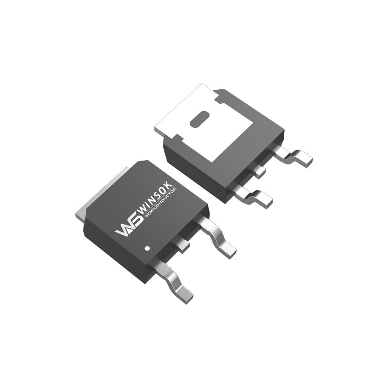
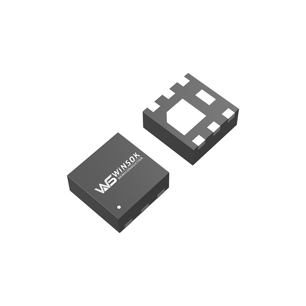
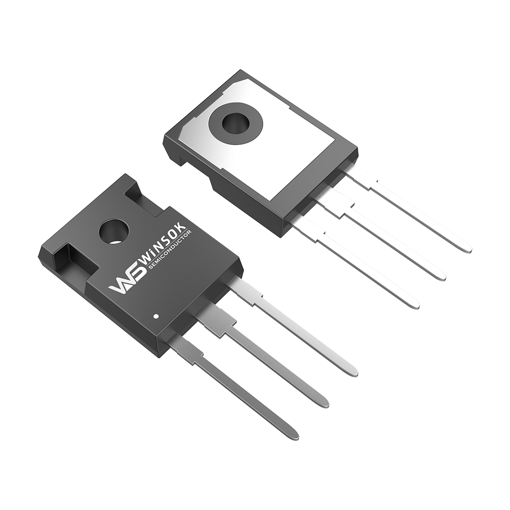
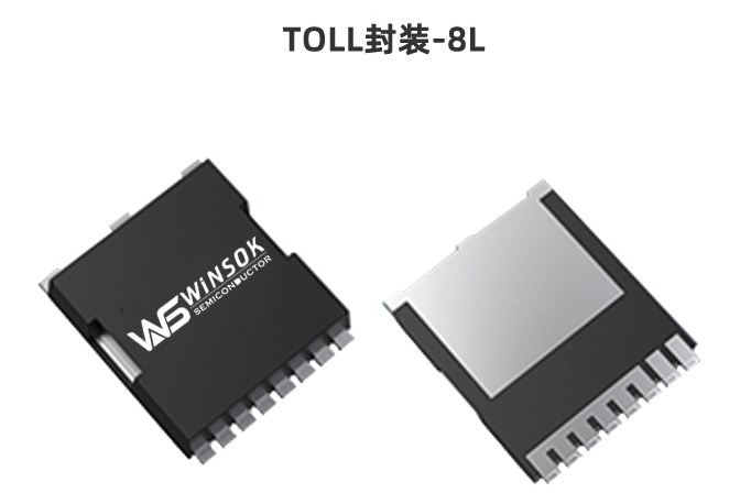
There are two major types of MOSFET: split junction type and insulated gate type. Junction MOSFET (JFET) is named because it has two PN junctions, and insulated gate MOSFET (JGFET) is named because the gate is completely insulated from other electrodes. At present, among insulated gate MOSFETs, the most commonly used one is MOSFET, referred to as MOSFET (metal-oxide-semiconductor MOSFET); in addition, there are PMOS, NMOS and VMOS power MOSFETs, as well as the recently launched πMOS and VMOS power modules, etc. .
According to the different channel semiconductor materials, junction type and insulating gate type are divided into channel and P channel. If divided according to conductivity mode, MOSFET can be divided into depletion type and enhancement type. Junction MOSFETs are all depletion type, and insulated gate MOSFETs are both depletion type and enhancement type.
Field effect transistors can be divided into junction field effect transistors and MOSFETs. MOSFETs are divided into four categories: N-channel depletion type and enhancement type; P-channel depletion type and enhancement type.
Characteristics of MOSFET
The characteristic of a MOSFET is the south gate voltage UG; which controls its drain current ID. Compared with ordinary bipolar transistors, MOSFETs have the characteristics of high input impedance, low noise, large dynamic range, low power consumption, and easy integration.
When the absolute value of the negative bias voltage (-UG) increases, the depletion layer increases, the channel decreases, and the drain current ID decreases. When the absolute value of the negative bias voltage (-UG) decreases, the depletion layer decreases, the channel increases, and the drain current ID increases. It can be seen that the drain current ID is controlled by the gate voltage, so the MOSFET is a voltage-controlled device, that is, the changes in the output current are controlled by changes in the input voltage, so as to achieve amplification and other purposes.
Like bipolar transistors, when MOSFET is used in circuits such as amplification, a bias voltage should also be added to its gate.
The gate of the junction field effect tube should be applied with a reverse bias voltage, that is, a negative gate voltage should be applied to the N-channel tube and a positive gate claw should be applied to the P-channel tube. Reinforced insulated gate MOSFET should apply forward gate voltage. The gate voltage of a depletion-mode insulating MOSFET can be positive, negative, or "0". The methods of adding bias include the fixed bias method, the self-supplied bias method, the direct coupling method, etc.
MOSFET has many parameters, including DC parameters, AC parameters and limit parameters, but in normal use, you only need to pay attention to the following main parameters: saturated drain-source current IDSS pinch-off voltage Up, (junction tube and depletion mode insulated gate tube, or turn-on Voltage UT (reinforced insulated gate tube), transconductance gm, drain-source breakdown voltage BUDS, maximum power dissipation PDSM and maximum drain-source current IDSM.
(1) Saturated drain-source current
The saturated drain-source current IDSS refers to the drain-source current when the gate voltage UGS=0 in a junction or depletion insulated gate MOSFET.
(2)Pinch-off voltage
The pinch-off voltage UP refers to the gate voltage when the drain-source connection is just cut off in a junction or depletion-type insulated gate MOSFET. As shown in 4-25 for the UGS-ID curve of the N-channel tube, the meaning of IDSS and UP can be clearly seen.
(3) Turn-on voltage
The turn-on voltage UT refers to the gate voltage when the drain-source connection is just made in the reinforced insulated gate MOSFET. Figure 4-27 shows the UGS-ID curve of the N-channel tube, and the meaning of UT can be clearly seen.
(4) Transconductance
Transconductance gm represents the ability of the gate-source voltage UGS to control the drain current ID, that is, the ratio of the change in the drain current ID to the change in the gate-source voltage UGS. 9m is an important parameter to measure the amplification capability of MOSFET.
(5)Drain-source breakdown voltage
The drain-source breakdown voltage BUDS refers to the maximum drain-source voltage that the MOSFET can accept when the gate-source voltage UGS is constant. This is a limiting parameter, and the operating voltage applied to the MOSFET must be less than BUDS.
(6)Maximum power dissipation
The maximum power dissipation PDSM is also a limit parameter, which refers to the maximum drain-source power dissipation allowed without deterioration of MOSFET performance. When used, the actual power consumption of MOSFET should be less than PDSM and leave a certain margin.
(7)Maximum drain-source current
The maximum drain-source current IDSM is another limit parameter, which refers to the maximum current allowed to pass between the drain and source when the MOSFET is operating normally. The operating current of the MOSFET should not exceed the IDSM.
1. MOSFET can be used for amplification. Since the input impedance of the MOSFET amplifier is very high, the coupling capacitor can be small and electrolytic capacitors do not have to be used.
2. The high input impedance of MOSFET is very suitable for impedance transformation. It is often used for impedance transformation in the input stage of multi-stage amplifiers.
3. MOSFET can be used as a variable resistor.
4. MOSFET can be conveniently used as a constant current source.
5. MOSFET can be used as an electronic switch.
MOSFET has the characteristics of low internal resistance, high withstand voltage, fast switching, and high avalanche energy. The designed current span is 1A-200A and the voltage span is 30V-1200V. We can adjust the electrical parameters according to the customer's application fields and application plans to improve customer Product reliability, overall conversion efficiency and product price competitiveness.
MOSFET vs Transistor Comparison
(1) MOSFET is a voltage control element, while a transistor is a current control element. When only a small amount of current is allowed to be taken from the signal source, a MOSFET should be used; when the signal voltage is low and a large amount of current is allowed to be taken from the signal source, a transistor should be used.
(2) MOSFET uses majority carriers to conduct electricity, so it is called a unipolar device, while transistors have both majority carriers and minority carriers to conduct electricity. It is called a bipolar device.
(3) The source and drain of some MOSFETs can be used interchangeably, and the gate voltage can be positive or negative, which is more flexible than transistors.
(4) MOSFET can work under very small current and very low voltage conditions, and its manufacturing process can easily integrate many MOSFETs on a silicon wafer. Therefore, MOSFETs have been widely used in large-scale integrated circuits.
How to judge the quality and polarity of MOSFET
Select the range of the multimeter to RX1K, connect the black test lead to the D pole, and the red test lead to the S pole. Touch the G and D poles at the same time with your hand. The MOSFET should be in an instantaneous conduction state, that is, the meter needle swings to a position with a smaller resistance. , and then touch the G and S poles with your hands, the MOSFET should have no response, that is, the meter needle will not move back to the zero position. At this time, it should be judged that the MOSFET is a good tube.
Select the range of the multimeter to RX1K, and measure the resistance between the three pins of the MOSFET. If the resistance between one pin and the other two pins is infinite, and it is still infinite after exchanging the test leads, Then this pin is the G pole, and the other two pins are the S pole and D pole. Then use a multimeter to measure the resistance value between the S pole and the D pole once, exchange the test leads and measure again. The one with the smaller resistance value is black. The test lead is connected to the S pole, and the red test lead is connected to the D pole.
MOSFET detection and usage precautions
1. Use a pointer multimeter to identify the MOSFET
1) Use resistance measurement method to identify the electrodes of junction MOSFET
According to the phenomenon that the forward and reverse resistance values of the PN junction of the MOSFET are different, the three electrodes of the junction MOSFET can be identified. Specific method: Set the multimeter to the R×1k range, select any two electrodes, and measure their forward and reverse resistance values respectively. When the forward and reverse resistance values of two electrodes are equal and are several thousand ohms, then the two electrodes are the drain D and the source S respectively. Because for junction MOSFETs, the drain and source are interchangeable, the remaining electrode must be the gate G. You can also touch the black test lead (red test lead is also acceptable) of the multimeter to any electrode, and the other test lead to touch the remaining two electrodes in sequence to measure the resistance value. When the resistance values measured twice are approximately equal, the electrode in contact with the black test lead is the gate, and the other two electrodes are the drain and source respectively. If the resistance values measured twice are both very large, it means that it is the reverse direction of the PN junction, that is, they are both reverse resistances. It can be determined that it is an N-channel MOSFET, and the black test lead is connected to the gate; if the resistance values measured twice are The resistance values are very small, indicating that it is a forward PN junction, that is, a forward resistance, and it is determined to be a P-channel MOSFET. The black test lead is also connected to the gate. If the above situation does not occur, you can replace the black and red test leads and conduct the test according to the above method until the grid is identified.
2) Use resistance measurement method to determine the quality of MOSFET
The resistance measurement method is to use a multimeter to measure the resistance between the MOSFET's source and drain, gate and source, gate and drain, gate G1 and gate G2 to determine whether it matches the resistance value indicated in the MOSFET manual. The management is good or bad. Specific method: First, set the multimeter to the R×10 or R×100 range, and measure the resistance between the source S and the drain D, usually in the range of tens of ohms to several thousand ohms (it can be seen in the manual that various models tubes, their resistance values are different), if the measured resistance value is greater than the normal value, it may be due to poor internal contact; if the measured resistance value is infinite, it may be an internal broken pole. Then set the multimeter to the R×10k range, and then measure the resistance values between gates G1 and G2, between the gate and the source, and between the gate and the drain. When the measured resistance values are all infinite, then It means that the tube is normal; if the above resistance values are too small or there is a path, it means that the tube is bad. It should be noted that if the two gates are broken in the tube, the component substitution method can be used for detection.
3) Use the induction signal input method to estimate the amplification capability of MOSFET
Specific method: Use the R×100 level of the multimeter resistance, connect the red test lead to the source S, and the black test lead to the drain D. Add a 1.5V power supply voltage to the MOSFET. At this time, the resistance value between the drain and the source is indicated by the meter needle. Then pinch the gate G of the junction MOSFET with your hand, and add the induced voltage signal of the human body to the gate. In this way, due to the amplification effect of the tube, the drain-source voltage VDS and the drain current Ib will change, that is, the resistance between the drain and the source will change. From this, it can be observed that the meter needle swings to a large extent. If the needle of the hand-held grid needle swings little, it means that the amplification ability of the tube is poor; if the needle swings greatly, it means that the amplification ability of the tube is large; if the needle does not move, it means that the tube is bad.
According to the above method, we use the R×100 scale of the multimeter to measure the junction MOSFET 3DJ2F. First open the G electrode of the tube and measure the drain-source resistance RDS to be 600Ω. After holding the G electrode with your hand, the meter needle swings to the left. The indicated resistance RDS is 12kΩ. If the meter needle swings larger, it means the tube is good. , and has greater amplification capability.
There are a few points to note when using this method: First, when testing the MOSFET and holding the gate with your hand, the multimeter needle may swing to the right (the resistance value decreases) or to the left (the resistance value increases). This is due to the fact that the AC voltage induced by the human body is relatively high, and different MOSFETs may have different working points when measured with a resistance range (either operating in the saturated zone or the unsaturated zone). Tests have shown that the RDS of most tubes increases. That is, the watch hand swings to the left; the RDS of a few tubes decreases, causing the watch hand to swing to the right.
But regardless of the direction in which the watch hand swings, as long as the watch hand swings larger, it means that the tube has greater amplification ability. Second, this method also works for MOSFETs. But it should be noted that the input resistance of MOSFET is high, and the allowed induced voltage of the gate G should not be too high, so do not pinch the gate directly with your hands. You must use the insulated handle of the screwdriver to touch the gate with a metal rod. , to prevent the charge induced by the human body from being directly added to the gate, causing gate breakdown. Third, after each measurement, the G-S poles should be short-circuited. This is because there will be a small amount of charge on the G-S junction capacitor, which builds up the VGS voltage. As a result, the hands of the meter may not move when measuring again. The only way to discharge the charge is to short-circuit the charge between the G-S electrodes.
4) Use resistance measurement method to identify unmarked MOSFETs
First, use the method of measuring resistance to find two pins with resistance values, namely the source S and the drain D. The remaining two pins are the first gate G1 and the second gate G2. Write down the resistance value between the source S and the drain D measured with two test leads first. Switch the test leads and measure again. Write down the measured resistance value. The one with the larger resistance value measured twice is the black test lead. The connected electrode is the drain D; the red test lead is connected to the source S. The S and D poles identified by this method can also be verified by estimating the amplification capability of the tube. That is, the black test lead with large amplification capability is connected to the D pole; the red test lead is connected to the ground to the 8-pole. The test results of both methods should be the same. After determining the positions of drain D and source S, install the circuit according to the corresponding positions of D and S. Generally, G1 and G2 will also be aligned in sequence. This determines the positions of the two gates G1 and G2. This determines the order of the D, S, G1, and G2 pins.
5) Use the change in reverse resistance value to determine the size of transconductance
When measuring the transconductance performance of VMOSN channel enhancement MOSFET, you can use the red test lead to connect the source S and the black test lead to the drain D. This is equivalent to adding a reverse voltage between the source and the drain. At this time, the gate is open circuit, and the reverse resistance value of the tube is very unstable. Select the ohm range of the multimeter to the high resistance range of R×10kΩ. At this time, the voltage in the meter is higher. When you touch the grid G with your hand, you will find that the reverse resistance value of the tube changes significantly. The greater the change, the higher the transconductance value of the tube; if the transconductance of the tube under test is very small, use this method to measure When , the reverse resistance changes little.
Precautions for using MOSFET
1) In order to use MOSFET safely, the limit values of parameters such as the dissipated power of the tube, the maximum drain-source voltage, the maximum gate-source voltage, and the maximum current cannot be exceeded in the circuit design.
2) When using various types of MOSFETs, they must be connected to the circuit in strict accordance with the required bias, and the polarity of the MOSFET bias must be observed. For example, there is a PN junction between the gate source and drain of a junction MOSFET, and the gate of an N-channel tube cannot be positively biased; the gate of a P-channel tube cannot be negatively biased, etc.
3) Because the input impedance of MOSFET is extremely high, the pins must be short-circuited during transportation and storage, and must be packaged with metal shielding to prevent external induced potential from breakdown of the gate. In particular, please note that MOSFET cannot be placed in a plastic box. It is best to store it in a metal box. At the same time, pay attention to keeping the tube moisture-proof.
4) In order to prevent MOSFET gate inductive breakdown, all test instruments, workbenches, soldering irons, and circuits themselves must be well grounded; when soldering the pins, solder the source first; before connecting to the circuit, the tube All lead ends should be short-circuited to each other, and the short-circuiting material should be removed after welding is completed; when removing the tube from the component rack, appropriate methods should be used to ensure that the human body is grounded, such as using a grounding ring; of course, if advanced A gas-heated soldering iron is more convenient for welding MOSFETs and ensures safety; the tube must not be inserted into or pulled out of the circuit before the power is turned off. The above safety measures must be paid attention to when using MOSFET.
5) When installing MOSFET, pay attention to the installation position and try to avoid being close to the heating element; in order to prevent the vibration of the pipe fittings, it is necessary to tighten the tube shell; when the pin leads are bent, they should be 5 mm larger than the root size to ensure that the Avoid bending the pins and causing air leakage.
For power MOSFETs, good heat dissipation conditions are required. Because power MOSFETs are used under high load conditions, sufficient heat sinks must be designed to ensure that the case temperature does not exceed the rated value so that the device can work stably and reliably for a long time.
In short, to ensure the safe use of MOSFETs, there are many things to pay attention to, and there are also various safety measures to be taken. The majority of professional and technical personnel, especially the majority of electronic enthusiasts, must proceed based on their actual situation and take Practical ways to use MOSFETs safely and effectively.


