


Understanding the operational principles of MOSFETs (Metal-Oxide-Semiconductor Field-Effect Transistors) is crucial for effectively utilizing these high-efficiency electronic components. MOSFETs are indispensable elements in electronic devices, and comprehending them is essential for manufacturers.
In practice, there are manufacturers who might not fully appreciate the specific functions of MOSFETs during their application. Nevertheless, by grasping the working principles of MOSFETs in electronic devices and their corresponding roles, one can strategically select the most suitable MOSFET, taking into account its unique characteristics and the specific traits of the product. This method enhances the performance of the product, bolstering its competitiveness in the market.
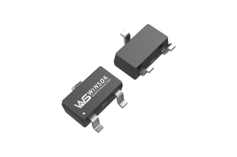
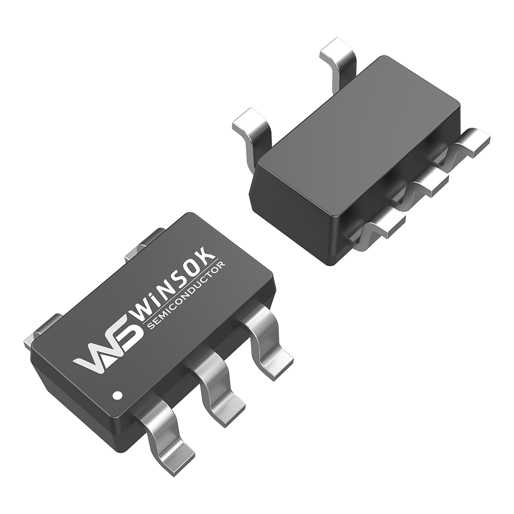
WINSOK SOT-23-3 package MOSFET
MOSFET Working Principles
When the gate-source voltage (VGS) of the MOSFET is zero, even with the application of a drain-source voltage (VDS), there is always a PN junction in reverse bias, resulting in no conductive channel (and no current) between the drain and source of the MOSFET. In this state, the drain current (ID) of the MOSFET is zero. Applying a positive voltage between the gate and source (VGS > 0) creates an electric field in the SiO2 insulating layer between the gate of the MOSFET and the silicon substrate, directed from the gate towards the P-type silicon substrate. Given that the oxide layer is insulating, the voltage applied to the gate, VGS, cannot generate a current in the MOSFET. Instead, it forms a capacitor across the oxide layer.
As VGS gradually increases, the capacitor charges up, creating an electric field. Attracted by the positive voltage at the gate, numerous electrons accumulate on the other side of the capacitor, forming an N-type conductive channel from the drain to the source in the MOSFET. When VGS exceeds the threshold voltage VT (typically around 2V), the N-channel of the MOSFET conducts, initiating the flow of drain current ID. The gate-source voltage at which the channel starts to form is referred to as the threshold voltage VT. By controlling the magnitude of VGS, and consequently the electric field, the size of the drain current ID in the MOSFET can be modulated.
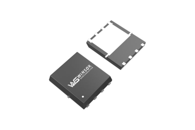
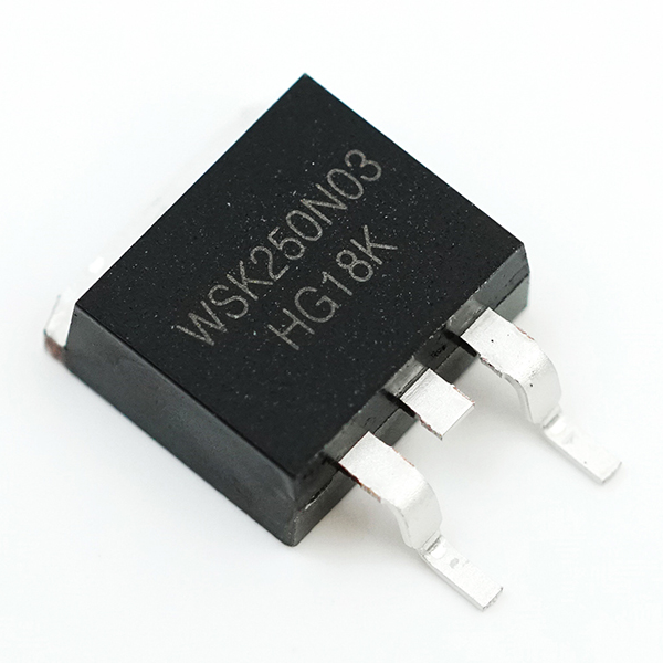
WINSOK DFN5x6-8 package MOSFET
MOSFET Applications
The MOSFET is renowned for its excellent switching characteristics, leading to its extensive application in circuits requiring electronic switches, such as switch-mode power supplies. In low-voltage applications using a 5V power supply, the use of traditional structures results in a voltage drop across the base-emitter of a bipolar junction transistor (about 0.7V), leaving only 4.3V for the final voltage applied to the gate of the MOSFET. In such scenarios, opting for a MOSFET with a nominal gate voltage of 4.5V introduces certain risks. This challenge also manifests in applications involving 3V or other low-voltage power supplies.
-

About MOSFET package type
-

How to determine whether a MOSFET is good or bad?
-

Which brand of MOSFET is good
-

MOSFET Operating Characteristics
-

Why are N channel MOSFET preferred over P chann...
-
MOSFET small current heating causes and measures
-
How to choose a MOSFET?
-
Introduction to the working principle of common...
-

Semiconductor Market Status of Electronic Infor...
-

Lithium battery charging is easy to damage, WIN...
-
What are the causes of inverter MOSFET heating?
-

What is a MOSFET? What are the main parameters?
-

Enabling High Power Applications: Winsok Mosfet...
-

Understanding the Operation and Modeling of MOS...
-
Olukey explains the parameters of MOSFET for you!
-
What are the causes of heat in the MOSFET of an...


