


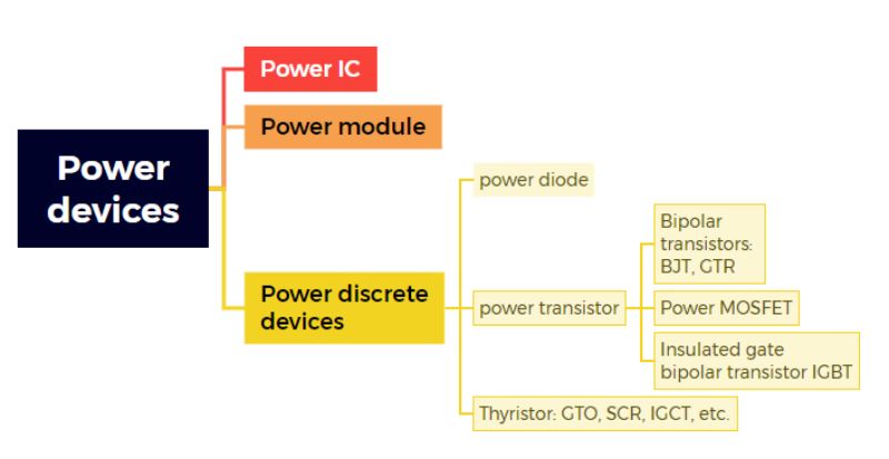
Power semiconductor devices are widely used in industry, consumption, military and other fields, and have a high strategic position. Let’s take a look at the overall picture of power devices from a picture:
Power semiconductor devices can be divided into full type, semi-controlled type and non-controllable type according to the degree of control of circuit signals. Or according to the signal properties of the driving circuit, it can be divided into voltage-driven type, current-driven type, etc.
| Classification | type | Specific power semiconductor devices |
| Controllability of electrical signals | Semi-controlled type | SCR |
| Full control | GTO、GTR,MOSFET、IGBT | |
| Uncontrollable | Power Diode | |
| Driving signal properties | Voltage driven type | IGBT、MOSFET、SITH |
| Current driven type | SCR、GTO、GTR | |
| Effective signal waveform | Pulse trigger type | SCR、GTO |
| Electronic control type | GTR、MOSFET、IGBT | |
| Situations in which current-carrying electrons participate | bipolar device | Power Diode、SCR、GTO、GTR、BSIT、BJT |
| Unipolar device | MOSFET、SIT | |
| Composite device | MCT, IGBT, SITH and IGCT |
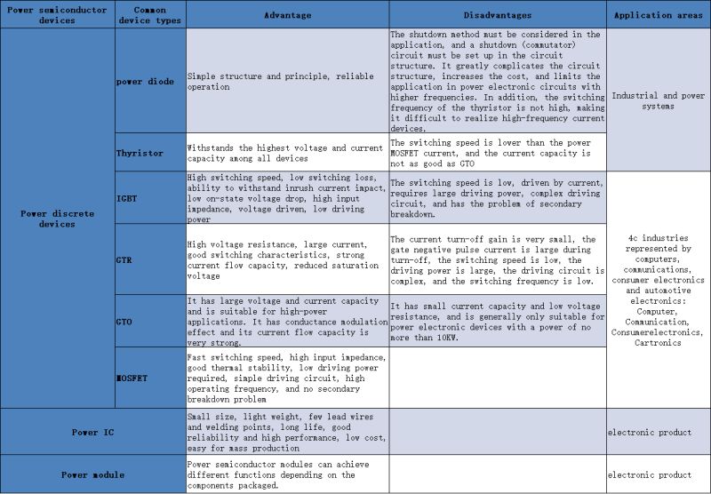
Different power semiconductor devices have different characteristics such as voltage, current capacity, impedance capability, and size. In actual use, appropriate devices need to be selected according to different fields and needs.
The semiconductor industry has gone through three generations of material changes since its birth. Up to now, the first semiconductor material represented by Si is still mainly used in the field of power semiconductor devices.
| Semiconductor material | Bandgap (eV) |
Melting point(K) | main application | |
| 1st generation semiconductor materials | Ge | 1.1 | 1221 | Low voltage, low frequency, medium power transistors, photodetectors |
| 2nd generation semiconductor materials | Si | 0.7 | 1687 | |
| 3rd generation semiconductor materials | GaAs | 1.4 | 1511 | Microwave, millimeter wave devices, light-emitting devices |
| SiC | 3.05 | 2826 | 1. High-temperature, high-frequency, radiation-resistant high-power devices 2. Blue, grade, violet light-emitting diodes, semiconductor lasers |
|
| GaN | 3.4 | 1973 | ||
| AIN | 6.2 | 2470 | ||
| C | 5.5 | >3800 | ||
| ZnO | 3.37 | 2248 | ||
Summarize the characteristics of semi-controlled and fully controlled power devices:
| Device type | SCR | GTR | MOSFET | IGBT |
| Control type | Pulse trigger | Current control | voltage control | film center |
| self-shutoff line | Commutation shutdown | self-shutdown device | self-shutdown device | self-shutdown device |
| working frequency | <1khz | <30khz | 20khz-Mhz | <40khz |
| Driving power | small | big | small | small |
| switching losses | big | big | big | big |
| conduction loss | small | small | big | small |
| Voltage and current level | 最大 | big | minimum | more |
| Typical applications | Medium frequency induction heating | UPS frequency converter | switching power supply | UPS frequency converter |
| price | lowest | lower | in the middle | The most expensive |
| conductance modulation effect | have | have | none | have |
Get to know MOSFETs
MOSFET has high input impedance, low noise, and good thermal stability; it has a simple manufacturing process and strong radiation, so it is usually used in amplifier circuits or switching circuits;
(1) Main selection parameters: drain-source voltage VDS (withstand voltage), ID continuous leakage current, RDS(on) on-resistance, Ciss input capacitance (junction capacitance), quality factor FOM=Ron*Qg, etc.
(2) According to different processes, it is divided into TrenchMOS: trench MOSFET, mainly in the low voltage field within 100V; SGT (Split Gate) MOSFET: split gate MOSFET, mainly in the medium and low voltage field within 200V; SJ MOSFET: super junction MOSFET, mainly in the High voltage field 600-800V;
In a switching power supply, such as an open-drain circuit, the drain is connected to the load intact, which is called an open-drain. In an open-drain circuit, no matter how high the voltage the load is connected, the load current can be turned on and off. It is an ideal analog switching device. This is the principle of MOSFET as a switching device.
In terms of market share, MOSFETs are almost all concentrated in the hands of major international manufacturers. Among them, Infineon acquired IR (American International Rectifier Company) in 2015 and became the industry leader. ON Semiconductor also completed the acquisition of Fairchild Semiconductor in September 2016. , the market share jumped to second place, and then the sales rankings were Renesas, Toshiba, IWC, ST, Vishay, Anshi, Magna, etc.;
Mainstream MOSFET brands are divided into several series: American, Japanese and Korean.
American series: Infineon, IR, Fairchild, ON Semiconductor, ST, TI, PI, AOS, etc.;
Japanese: Toshiba, Renesas, ROHM, etc.;
Korean series: Magna, KEC, AUK, Morina Hiroshi, Shinan, KIA
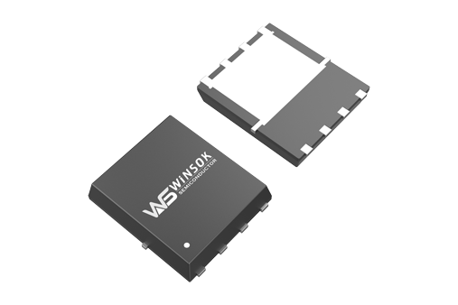
MOSFET package categories
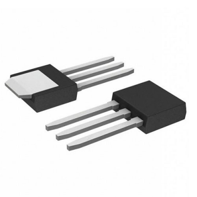
According to the way it is installed on the PCB board, there are two main types of MOSFET packages: plug-in (Through Hole) and surface mount (Surface Mount).
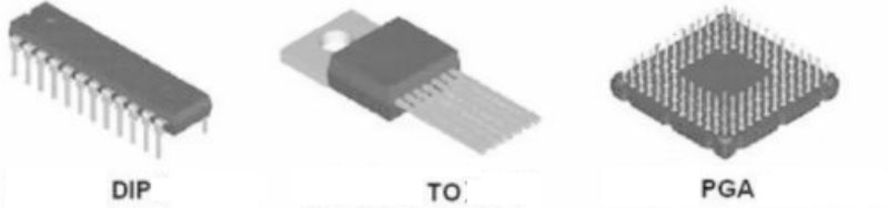
The plug-in type means that the pins of the MOSFET pass through the mounting holes of the PCB board and are welded to the PCB board. Common plug-in packages include: dual in-line package (DIP), transistor outline package (TO), and pin grid array package (PGA).
Plug-in packaging
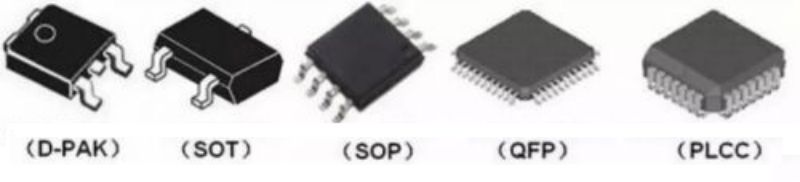
Surface mounting is where the MOSFET pins and heat dissipation flange are welded to the pads on the surface of the PCB board. Typical surface mount packages include: transistor outline (D-PAK), small outline transistor (SOT), small outline package (SOP), quad flat package (QFP), plastic leaded chip carrier (PLCC), etc.
surface mount package
With the development of technology, PCB boards such as motherboards and graphics cards currently use less and less direct plug-in packaging, and more surface mount packaging is used.
1. Dual in-line package (DIP)
The DIP package has two rows of pins and needs to be inserted into a chip socket with a DIP structure. Its derivation method is SDIP (Shrink DIP), which is a shrink double-in-line package. The pin density is 6 times higher than that of DIP.
DIP packaging structure forms include: multi-layer ceramic dual-in-line DIP, single-layer ceramic dual-in-line DIP, lead frame DIP (including glass-ceramic sealing type, plastic encapsulation structure type, ceramic low-melting glass encapsulation type) etc. The characteristic of DIP packaging is that it can easily realize through-hole welding of PCB boards and has good compatibility with the motherboard.
However, because its packaging area and thickness are relatively large, and the pins are easily damaged during the plugging and unplugging process, the reliability is poor. At the same time, due to the influence of the process, the number of pins generally does not exceed 100. Therefore, in the process of high integration of the electronic industry, DIP packaging has gradually withdrawn from the stage of history.
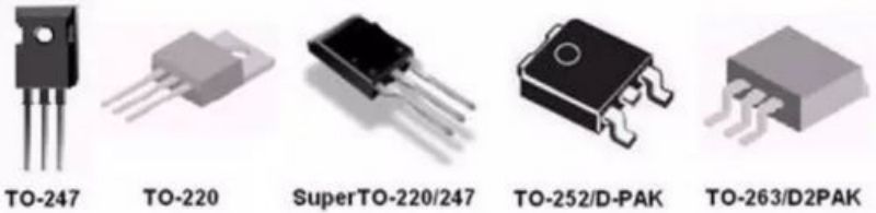
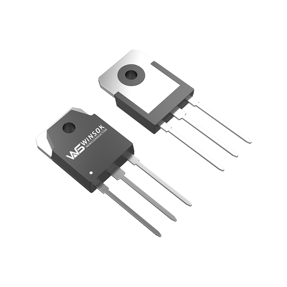
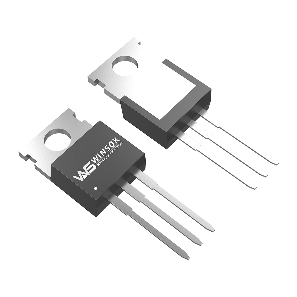
2. Transistor Outline Package (TO)
Early packaging specifications, such as TO-3P, TO-247, TO-92, TO-92L, TO-220, TO-220F, TO-251, etc. are all plug-in packaging designs.
TO-3P/247: It is a commonly used packaging form for medium-high voltage and high-current MOSFETs. The product has the characteristics of high withstand voltage and strong breakdown resistance.
TO-220/220F: TO-220F is a fully plastic package, and there is no need to add an insulating pad when installing it on a radiator; TO-220 has a metal sheet connected to the middle pin, and an insulating pad is required when installing the radiator. The MOSFETs of these two package styles have similar appearances and can be used interchangeably.
TO-251: This packaged product is mainly used to reduce costs and reduce product size. It is mainly used in environments with medium voltage and high current below 60A and high voltage below 7N.
TO-92: This package is only used for low-voltage MOSFET (current below 10A, withstand voltage below 60V) and high-voltage 1N60/65, in order to reduce costs.
In recent years, due to the high welding cost of the plug-in packaging process and inferior heat dissipation performance to patch-type products, the demand in the surface mount market has continued to increase, which has also led to the development of TO packaging into surface mount packaging.
TO-252 (also called D-PAK) and TO-263 (D2PAK) are both surface mount packages.。
TO package product appearance
TO252/D-PAK is a plastic chip package, which is commonly used for packaging power transistors and voltage stabilizing chips. It is one of the current mainstream packages. The MOSFET using this packaging method has three electrodes, gate (G), drain (D), and source (S). The drain (D) pin is cut off and not used. Instead, the heat sink on the back is used as the drain (D), which is directly welded to the PCB. On the one hand, it is used to output large currents, and on the other hand, it dissipates heat through the PCB. Therefore, there are three D-PAK pads on the PCB, and the drain (D) pad is larger. Its packaging specifications are as follows:
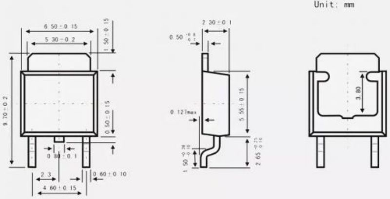
TO-252/D-PAK package size specifications
TO-263 is a variant of TO-220. It is mainly designed to improve production efficiency and heat dissipation. It supports extremely high current and voltage. It is more common in medium-voltage high-current MOSFETs below 150A and above 30V. In addition to D2PAK (TO-263AB), it also includes TO263-2, TO263-3, TO263-5, TO263-7 and other styles, which are subordinate to TO-263, mainly due to the different number and distance of pins.
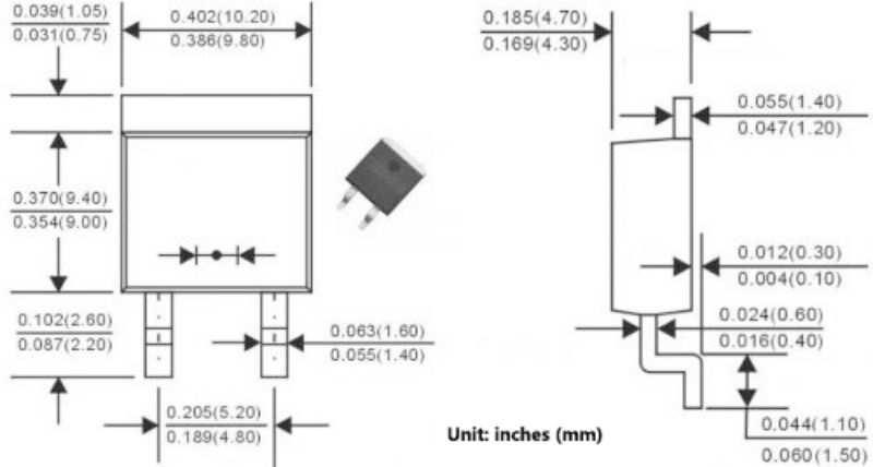
TO-263/D2PAK package size specifications
3. Pin grid array package (PGA)
There are multiple square array pins inside and outside the PGA (Pin Grid Array Package) chip. Each square array pin is arranged at a certain distance around the chip. Depending on the number of pins, it can be formed into 2 to 5 circles. During installation, just insert the chip into the special PGA socket. It has the advantages of easy plugging and unplugging and high reliability, and can adapt to higher frequencies.
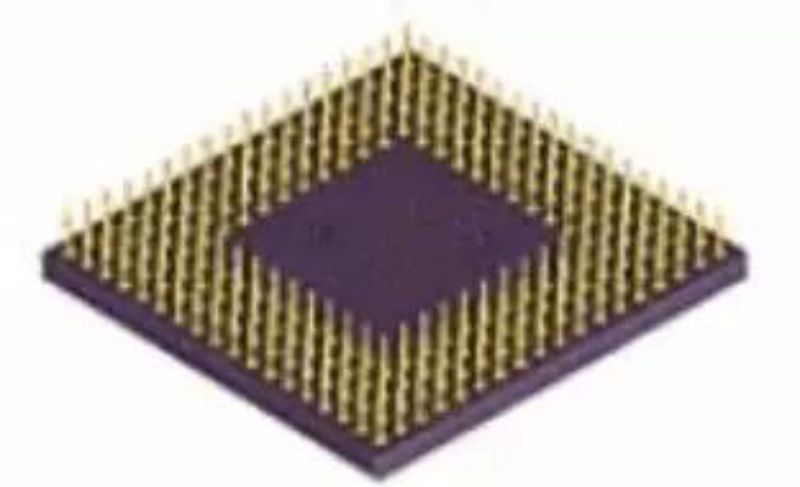
PGA package style
Most of its chip substrates are made of ceramic material, and some use special plastic resin as the substrate. In terms of technology, the pin center distance is usually 2.54mm, and the number of pins ranges from 64 to 447. The characteristic of this kind of packaging is that the smaller the packaging area (volume), the lower the power consumption (performance) it can withstand, and vice versa. This packaging style of chips was more common in the early days, and was mostly used for packaging high-power consumption products such as CPUs. For example, Intel's 80486 and Pentium all use this packaging style; it is not widely adopted by MOSFET manufacturers.
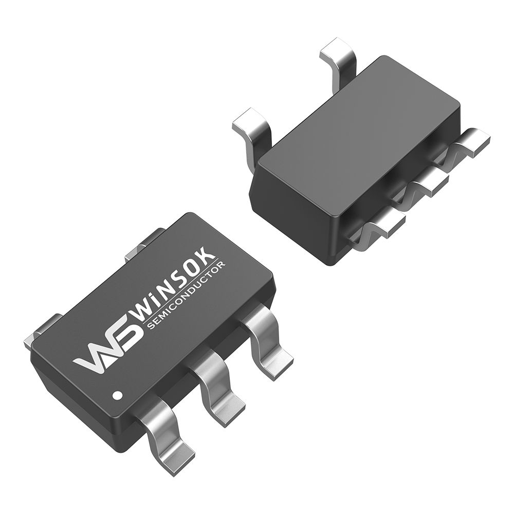
4. Small Outline Transistor Package (SOT)
SOT (Small Out-Line Transistor) is a patch type small power transistor package, mainly including SOT23, SOT89, SOT143, SOT25 (ie SOT23-5), etc. SOT323, SOT363/SOT26 (i.e. SOT23-6) and other types are derived, which are smaller in size than TO packages.
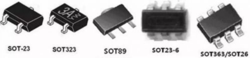
SOT package type
SOT23 is a commonly used transistor package with three wing-shaped pins, namely collector, emitter and base, which are listed on both sides of the long side of the component. Among them, the emitter and base are on the same side. They are common in low-power transistors, field effect transistors and composite transistors with resistor networks. They have good strength but poor solderability. The appearance is shown in Figure (a) below.
SOT89 has three short pins distributed on one side of the transistor. The other side is a metal heat sink connected to the base to increase heat dissipation capability. It is common in silicon power surface mount transistors and is suitable for higher power applications. The appearance is shown in Figure (b) below.
SOT143 has four short wing-shaped pins, which are led out from both sides. The wider end of the pin is the collector. This type of package is common in high-frequency transistors, and its appearance is shown in Figure (c) below.
SOT252 is a high-power transistor with three pins leading from one side, and the middle pin is shorter and is the collector. Connect to the larger pin at the other end, which is a copper sheet for heat dissipation, and its appearance is as shown in Figure (d) below.
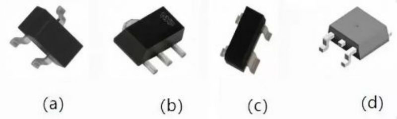
Common SOT package appearance comparison
The four-terminal SOT-89 MOSFET is commonly used on motherboards. Its specifications and dimensions are as follows:
SOT-89 MOSFET size specifications (unit: mm)
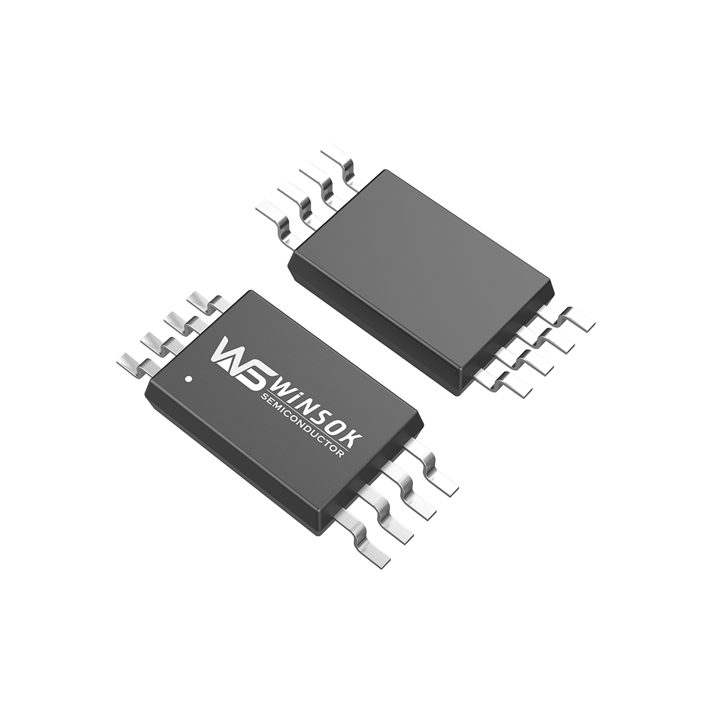
5. Small Outline Package (SOP)
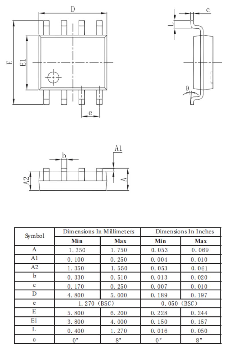
SOP (Small Out-Line Package) is one of the surface mount packages, also called SOL or DFP. The pins are drawn out from both sides of the package in a seagull wing shape (L shape). The materials are plastic and ceramic. SOP packaging standards include SOP-8, SOP-16, SOP-20, SOP-28, etc. The number after SOP indicates the number of pins. Most MOSFET SOP packages adopt SOP-8 specifications. The industry often omits "P" and abbreviates it as SO (Small Out-Line).
SOP-8 package size
SO-8 was first developed by PHILIP Company. It is packaged in plastic, has no heat dissipation bottom plate, and has poor heat dissipation. It is generally used for low-power MOSFETs. Later, standard specifications such as TSOP (Thin Small Outline Package), VSOP (Very Small Outline Package), SSOP (Shrink SOP), TSSOP (Thin Shrink SOP), etc. were gradually derived; among them, TSOP and TSSOP are commonly used in MOSFET packaging.
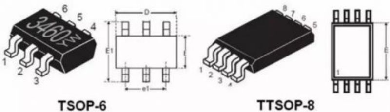
SOP derived specifications commonly used for MOSFETs
6. Quad Flat Package (QFP)
The distance between chip pins in QFP (Plastic Quad Flat Package) package is very small and the pins are very thin. It is generally used in large-scale or ultra-large integrated circuits, and the number of pins is generally more than 100. Chips packaged in this form must use SMT surface mounting technology to solder the chip to the motherboard. This packaging method has four major characteristics: ① It is suitable for SMD surface mounting technology to install wiring on PCB circuit boards; ② It is suitable for high-frequency use; ③ It is easy to operate and has high reliability; ④ The ratio between the chip area and the packaging area is small. Like the PGA packaging method, this packaging method wraps the chip in a plastic package and cannot dissipate the heat generated when the chip is working in a timely manner. It restricts the improvement of MOSFET performance; and the plastic packaging itself increases the size of the device, which does not meet the requirements for the development of semiconductors in the direction of being light, thin, short, and small. In addition, this type of packaging method is based on a single chip, which has the problems of low production efficiency and high packaging cost. Therefore, QFP is more suitable for use in digital logic LSI circuits such as microprocessors/gate arrays, and is also suitable for packaging analog LSI circuit products such as VTR signal processing and audio signal processing.
7、Quad flat package with no leads (QFN)
The QFN (Quad Flat Non-leaded package) package is equipped with electrode contacts on all four sides. Since there are no leads, the mounting area is smaller than QFP and the height is lower than QFP. Among them, ceramic QFN is also called LCC (Leadless Chip Carriers), and low-cost plastic QFN using glass epoxy resin printed substrate base material is called plastic LCC, PCLC, P-LCC, etc. It is an emerging surface mount chip packaging technology with small pad size, small volume, and plastic as sealing material. QFN is mainly used for integrated circuit packaging, and MOSFET will not be used. However, because Intel proposed an integrated driver and MOSFET solution, it launched DrMOS in a QFN-56 package ("56" refers to the 56 connection pins on the back of the chip).
It should be noted that the QFN package has the same external lead configuration as the ultra-thin small outline package (TSSOP), but its size is 62% smaller than the TSSOP. According to QFN modeling data, its thermal performance is 55% higher than that of TSSOP packaging, and its electrical performance (inductance and capacitance) are 60% and 30% higher than TSSOP packaging respectively. The biggest disadvantage is that it is difficult to repair.
DrMOS in QFN-56 package
Traditional discrete DC/DC step-down switching power supplies cannot meet the requirements for higher power density, nor can they solve the problem of parasitic parameter effects at high switching frequencies. With the innovation and progress of technology, it has become a reality to integrate drivers and MOSFETs to build multi-chip modules. This integration method can save considerable space and increase power consumption density. Through the optimization of drivers and MOSFETs, it has become a reality. Power efficiency and high-quality DC current, this is DrMOS integrated driver IC.
Renesas 2nd generation DrMOS
The QFN-56 leadless package makes DrMOS thermal impedance very low; with internal wire bonding and copper clip design, external PCB wiring can be minimized, thereby reducing inductance and resistance. In addition, the deep-channel silicon MOSFET process used can also significantly reduce conduction, switching and gate charge losses; it is compatible with a variety of controllers, can achieve different operating modes, and supports active phase conversion mode APS (Auto Phase Switching). In addition to QFN packaging, bilateral flat no-lead packaging (DFN) is also a new electronic packaging process that has been widely used in various components of ON Semiconductor. Compared with QFN, DFN has fewer lead-out electrodes on both sides.
8、Plastic Leaded Chip Carrier (PLCC)
PLCC (Plastic Quad Flat Package) has a square shape and is much smaller than the DIP package. It has 32 pins with pins all around. The pins are led out from the four sides of the package in a T-shape. It is a plastic product. The pin center distance is 1.27mm, and the number of pins ranges from 18 to 84. The J-shaped pins are not easily deformed and are easier to operate than QFP, but the appearance inspection after welding is more difficult. PLCC packaging is suitable for installing wiring on PCB using SMT surface mounting technology. It has the advantages of small size and high reliability. PLCC packaging is relatively common and is used in logic LSI, DLD (or program logic device) and other circuits. This packaging form is often used in motherboard BIOS, but it is currently less common in MOSFETs.
Encapsulation and improvement for mainstream enterprises
Due to the development trend of low voltage and high current in CPUs, MOSFETs are required to have large output current, low on-resistance, low heat generation, fast heat dissipation, and small size. In addition to improving chip production technology and processes, MOSFET manufacturers also continue to improve packaging technology. On the basis of compatibility with standard appearance specifications, they propose new packaging shapes and register trademark names for the new packages they develop.
1、RENESAS WPAK, LFPAK and LFPAK-I packages
WPAK is a high heat radiation package developed by Renesas. By imitating the D-PAK package, the chip heat sink is welded to the motherboard, and the heat is dissipated through the motherboard, so that the small package WPAK can also reach the output current of D-PAK. WPAK-D2 packages two high/low MOSFETs to reduce wiring inductance.
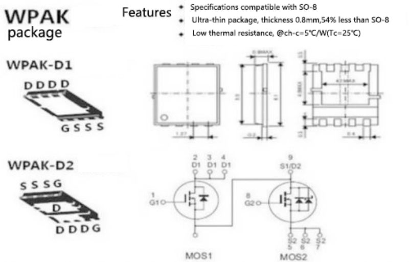
Renesas WPAK package size
LFPAK and LFPAK-I are two other small form-factor packages developed by Renesas that are compatible with SO-8. LFPAK is similar to D-PAK, but smaller than D-PAK. LFPAK-i places the heat sink upwards to dissipate heat through the heat sink.
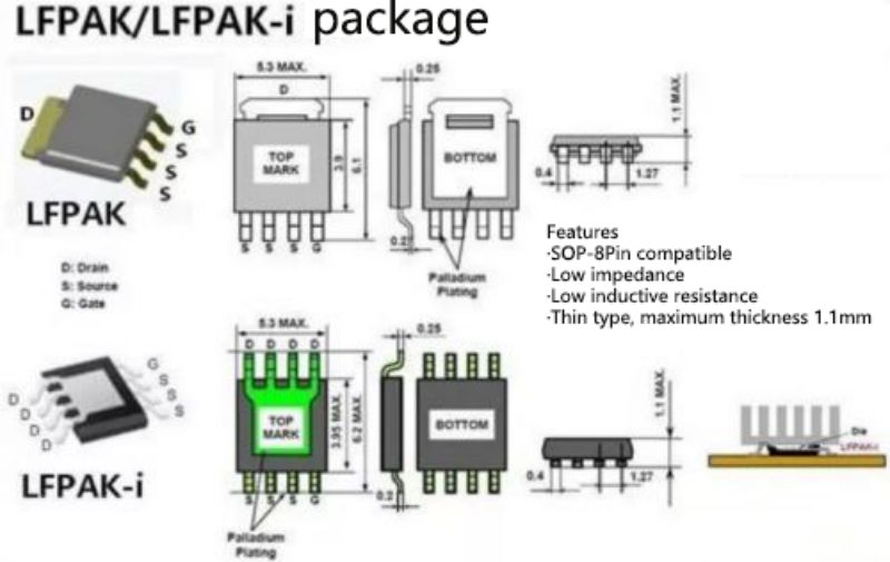
Renesas LFPAK and LFPAK-I packages
2. Vishay Power-PAK and Polar-PAK packaging
Power-PAK is the MOSFET package name registered by Vishay Corporation. Power-PAK includes two specifications: Power-PAK1212-8 and Power-PAK SO-8.
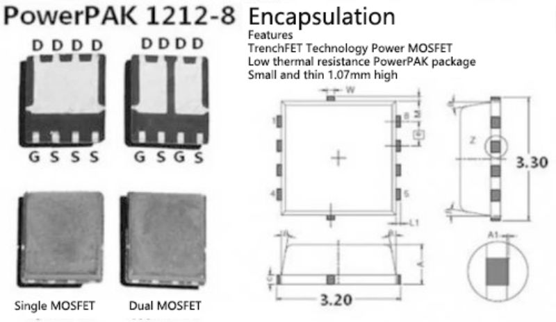
Vishay Power-PAK1212-8 package
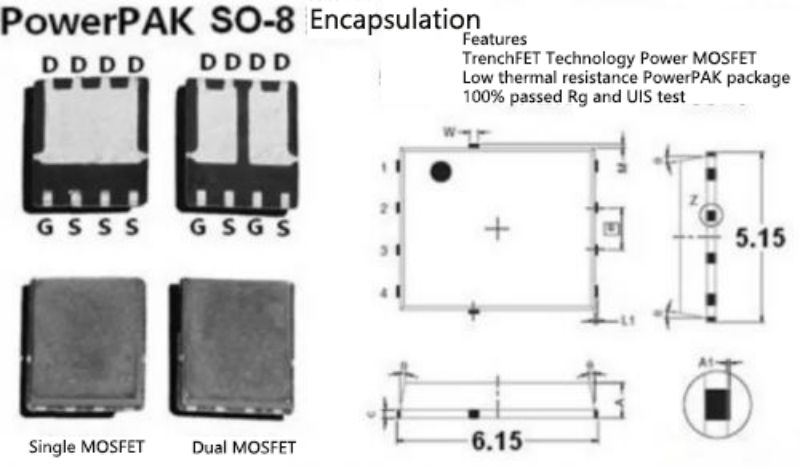
Vishay Power-PAK SO-8 package
Polar PAK is a small package with double-sided heat dissipation and is one of Vishay's core packaging technologies. Polar PAK is the same as the ordinary so-8 package. It has dissipation points on both the upper and lower sides of the package. It is not easy to accumulate heat inside the package and can increase the current density of the operating current to twice that of SO-8. Currently, Vishay has licensed Polar PAK technology to STMicroelectronics.
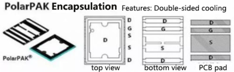
Vishay Polar PAK package
3. Onsemi SO-8 and WDFN8 flat lead packages
ON Semiconductor has developed two types of flat-lead MOSFETs, among which the SO-8 compatible flat-lead ones are used by many boards. ON Semiconductor's newly launched NVMx and NVTx power MOSFETs use compact DFN5 (SO-8FL) and WDFN8 packages to minimize conduction losses. It also features low QG and capacitance to minimize driver losses.
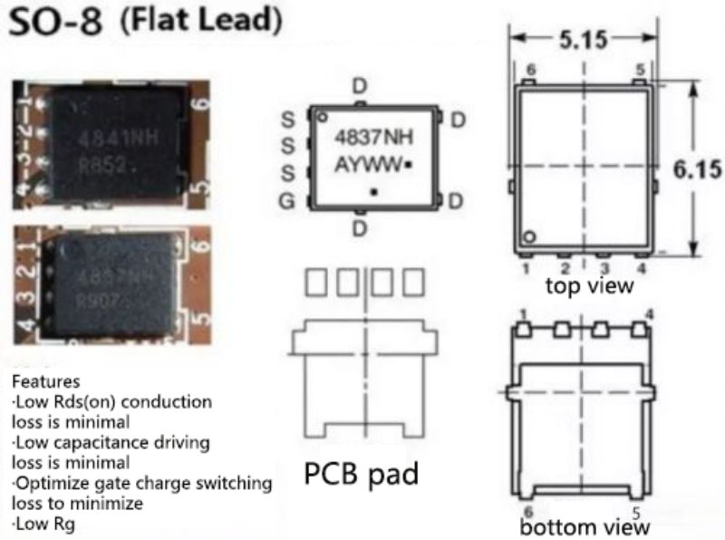
ON Semiconductor SO-8 Flat Lead Package
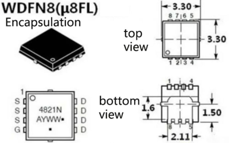
ON Semiconductor WDFN8 package
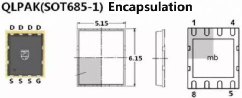
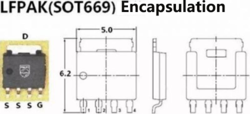
4. NXP LFPAK and QLPAK packaging
NXP (formerly Philps) has improved SO-8 packaging technology into LFPAK and QLPAK. Among them, LFPAK is considered to be the most reliable power SO-8 package in the world; while QLPAK has the characteristics of small size and higher heat dissipation efficiency. Compared with ordinary SO-8, QLPAK occupies a PCB board area of 6*5mm and has a thermal resistance of 1.5k/W.
NXP LFPAK package
NXP QLPAK packaging
4. ST Semiconductor PowerSO-8 package
STMicroelectronics’ power MOSFET chip packaging technologies include SO-8, PowerSO-8, PowerFLAT, DirectFET, PolarPAK, etc. Among them, Power SO-8 is an improved version of SO-8. In addition, there are PowerSO-10, PowerSO-20, TO-220FP, H2PAK-2 and other packages.

STMicroelectronics Power SO-8 package
5. Fairchild Semiconductor Power 56 package
Power 56 is Farichild's exclusive name, and its official name is DFN5×6. Its packaging area is comparable to that of the commonly used TSOP-8, and the thin package saves component clearance height, and the Thermal-Pad design at the bottom reduces thermal resistance. Therefore, many power device manufacturers have deployed DFN5×6.
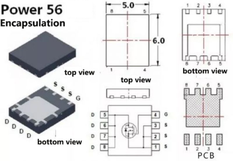
Fairchild Power 56 package
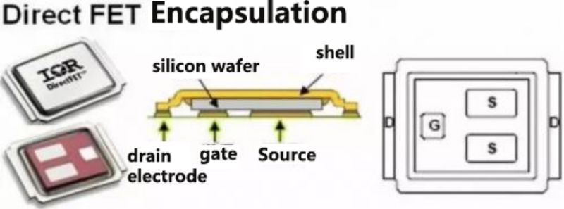
6. International Rectifier (IR) Direct FET package
Direct FET provides efficient upper cooling in an SO-8 or smaller footprint and is suitable for AC-DC and DC-DC power conversion applications in computers, laptops, telecommunications and consumer electronics equipment. DirectFET's metal can construction provides double-sided heat dissipation, effectively doubling the current handling capabilities of high-frequency DC-DC buck converters compared to standard plastic discrete packages. The Direct FET package is a reverse-mounted type, with the drain (D) heat sink facing upwards and covered with a metal shell, through which heat is dissipated. Direct FET packaging greatly improves heat dissipation and takes up less space with good heat dissipation.
Summarize
In the future, as the electronic manufacturing industry continues to develop in the direction of ultra-thin, miniaturization, low voltage, and high current, the appearance and internal packaging structure of MOSFET will also change to better adapt to the development needs of the manufacturing industry. In addition, in order to lower the selection threshold for electronic manufacturers, the trend of MOSFET development in the direction of modularization and system-level packaging will become increasingly obvious, and products will develop in a coordinated manner from multiple dimensions such as performance and cost. Package is one of the important reference factors for MOSFET selection. Different electronic products have different electrical requirements, and different installation environments also require matching size specifications to meet. In actual selection, the decision should be made according to the actual needs under the general principle. Some electronic systems are limited by the size of the PCB and internal height. For example, module power supplies of communication systems usually use DFN5*6 and DFN3*3 packages due to height restrictions; in some ACDC power supplies, ultra-thin designs or due to shell limitations are suitable for assembling TO220 packaged power MOSFETs. At this time, the pins can be directly inserted into the root, which is not suitable for TO247 packaged products; some ultra-thin designs require the device pins to be bent and laid flat, which will increase the complexity of MOSFET selection.
How to choose MOSFET
An engineer once told me that he never looked at the first page of a MOSFET data sheet because the "practical" information only appeared on the second page and beyond. Virtually every page on a MOSFET data sheet contains valuable information for designers. But it's not always clear how to interpret the data provided by manufacturers.
This article outlines some of the key specifications of MOSFETs, how they are stated on the datasheet, and the clear picture you need to understand them. Like most electronic devices, MOSFETs are affected by operating temperature. So it is important to understand the test conditions under which the mentioned indicators are applied. It is also crucial to understand whether the indicators you see in the "Product Introduction" are "maximum" or "typical" values, because some data sheets do not make it clear.
Voltage grade
The primary characteristic that determines a MOSFET is its drain-source voltage VDS, or "drain-source breakdown voltage", which is the highest voltage that the MOSFET can withstand without damage when the gate is short-circuited to the source and the drain current is 250μA. . VDS is also called the "absolute maximum voltage at 25°C", but it is important to remember that this absolute voltage is temperature dependent, and there is usually a "VDS temperature coefficient" in the data sheet. You also need to understand that maximum VDS is the DC voltage plus any voltage spikes and ripples that may be present in the circuit. For example, if you use a 30V device on a 30V power supply with a 100mV, 5ns spike, the voltage will exceed the absolute maximum limit of the device and the device may enter avalanche mode. In this case, the reliability of the MOSFET cannot be guaranteed. At high temperatures, the temperature coefficient can significantly change the breakdown voltage. For example, some N-channel MOSFETs with a voltage rating of 600V have a positive temperature coefficient. As they approach their maximum junction temperature, the temperature coefficient causes these MOSFETs to behave like 650V MOSFETs. Many MOSFET users' design rules require a derating factor of 10% to 20%. In some designs, considering that the actual breakdown voltage is 5% to 10% higher than the rated value at 25°C, a corresponding useful design margin will be added to the actual design, which is very beneficial to the design. Equally important to the correct selection of MOSFETs is understanding the role of the gate-source voltage VGS during the conduction process. This voltage is the voltage that ensures full conduction of the MOSFET under a given maximum RDS(on) condition. This is why the on-resistance is always related to the VGS level, and it is only at this voltage that the device can be turned on. An important design consequence is that you cannot turn the MOSFET fully on with a voltage lower than the minimum VGS used to achieve the RDS(on) rating. For example, to drive a MOSFET fully on with a 3.3V microcontroller, you need to be able to turn on the MOSFET at VGS=2.5V or lower.
On-resistance, gate charge, and "figure of merit"
The on-resistance of a MOSFET is always determined at one or more gate-to-source voltages. The maximum RDS(on) limit can be 20% to 50% higher than the typical value. The maximum limit of RDS(on) usually refers to the value at a junction temperature of 25°C. At higher temperatures, RDS(on) can increase by 30% to 150%, as shown in Figure 1. Since RDS(on) changes with temperature and the minimum resistance value cannot be guaranteed, detecting current based on RDS(on) is not a very accurate method.

Figure 1 RDS(on) increases with temperature in the range of 30% to 150% of the maximum operating temperature
On-resistance is very important for both N-channel and P-channel MOSFETs. In switching power supplies, Qg is a key selection criterion for N-channel MOSFETs used in switching power supplies because Qg affects switching losses. These losses have two effects: one is the switching time that affects the MOSFET on and off; the other is the energy required to charge the gate capacitance during each switching process. One thing to keep in mind is that Qg depends on the gate-source voltage, even if using a lower Vgs reduces switching losses. As a quick way to compare MOSFETs intended for use in switching applications, designers often use a singular formula consisting of RDS(on) for conduction losses and Qg for switching losses: RDS(on)xQg. This "figure of merit" (FOM) summarizes the device's performance and allows MOSFETs to be compared in terms of typical or maximum values. To ensure an accurate comparison across devices, you need to make sure that the same VGS is used for RDS(on) and Qg, and that the typical and maximum values do not happen to be mixed together in the publication. Lower FOM will give you better performance in switching applications, but it's not guaranteed. The best comparison results can only be obtained in an actual circuit, and in some cases the circuit may need to be fine-tuned for each MOSFET. Rated current and power dissipation, based on different test conditions, most MOSFETs have one or more continuous drain currents in the data sheet. You'll want to look at the data sheet carefully to figure out whether the rating is at the specified case temperature (e.g. TC=25°C), or ambient temperature (e.g. TA=25°C). Which of these values is most relevant will depend on the device characteristics and application (see Figure 2).
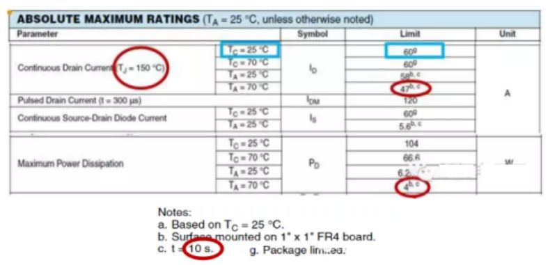
Figure 2 All absolute maximum current and power values are real data
For small surface mount devices used in handheld devices, the most relevant current level may be that at an ambient temperature of 70°C. For large equipment with heat sinks and forced air cooling, the current level at TA=25℃ may be closer to the actual situation. For some devices, the die can handle more current at its maximum junction temperature than the package limits. In some data sheets, this "die-limited" current level is additional information to the "package-limited" current level, which can give you an idea of the robustness of the die. Similar considerations apply to continuous power dissipation, which depends not only on temperature but also on-time. Imagine a device operating continuously at PD=4W for 10 seconds at TA=70℃. What constitutes a "continuous" time period will vary based on the MOSFET package, so you'll want to use the normalized thermal transient impedance plot from the datasheet to see what the power dissipation looks like after 10 seconds, 100 seconds, or 10 minutes. As shown in Figure 3, the thermal resistance coefficient of this specialized device after a 10-second pulse is approximately 0.33, which means that once the package reaches thermal saturation after approximately 10 minutes, the device's heat dissipation capacity is only 1.33W instead of 4W. Although the heat dissipation capacity of the device can reach about 2W under good cooling.
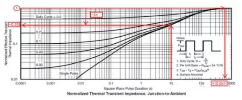
Figure 3 Thermal resistance of MOSFET when power pulse is applied
In fact, we can divide how to choose MOSFET into four steps.
The first step: choose N channel or P channel
The first step in choosing the right device for your design is deciding whether to use an N-channel or P-channel MOSFET. In a typical power application, when a MOSFET is connected to ground and the load is connected to the mains voltage, the MOSFET forms the low-side switch. In the low-side switch, N-channel MOSFETs should be used due to considerations of the voltage required to turn the device off or on. When the MOSFET is connected to the bus and load to ground, a high-side switch is used. P-channel MOSFETs are usually used in this topology, which is also due to voltage drive considerations. To select the right device for your application, you must determine the voltage required to drive the device and the easiest way to do it in your design. The next step is to determine the required voltage rating, or the maximum voltage the device can withstand. The higher the voltage rating, the higher the cost of the device. According to practical experience, the rated voltage should be greater than the mains voltage or bus voltage. This will provide sufficient protection so that the MOSFET will not fail. When selecting a MOSFET, it is necessary to determine the maximum voltage that can be tolerated from the drain to the source, that is, the maximum VDS. It is important to know that the maximum voltage a MOSFET can withstand changes with temperature. Designers must test voltage variations over the entire operating temperature range. The rated voltage must have enough margin to cover this variation range to ensure that the circuit will not fail. Other safety factors that design engineers need to consider include voltage transients induced by switching electronics such as motors or transformers. Rated voltages vary for different applications; typically, 20V for portable devices, 20-30V for FPGA power supplies, and 450-600V for 85-220VAC applications.
Step 2: Determine the rated current
The second step is to choose the current rating of the MOSFET. Depending on the circuit configuration, this rated current should be the maximum current that the load can withstand under all circumstances. Similar to the voltage situation, the designer must ensure that the MOSFET selected can withstand this current rating, even when the system generates current spikes. The two current conditions considered are continuous mode and pulse spike. In continuous conduction mode, the MOSFET is in a steady state, where current flows continuously through the device. A pulse spike refers to a large surge (or spike current) flowing through the device. Once the maximum current under these conditions is determined, it is simply a matter of selecting a device that can handle this maximum current. After selecting the rated current, the conduction loss must also be calculated. In actual situations, MOSFET is not an ideal device because there is electrical energy loss during the conduction process, which is called conduction loss. A MOSFET behaves like a variable resistor when "on", which is determined by the RDS(ON) of the device and changes significantly with temperature. The power loss of the device can be calculated by Iload2×RDS(ON). Since the on-resistance changes with temperature, the power loss will also change proportionally. The higher the voltage VGS applied to the MOSFET, the smaller the RDS(ON) will be; conversely, the higher the RDS(ON) will be. For the system designer, this is where the trade-offs come in depending on the system voltage. For portable designs, it is easier (and more common) to use lower voltages, while for industrial designs, higher voltages can be used. Note that the RDS(ON) resistance will rise slightly with current. Variations in various electrical parameters of the RDS(ON) resistor can be found in the technical data sheet provided by the manufacturer. Technology has a significant impact on device characteristics, because some technologies tend to increase RDS(ON) when increasing the maximum VDS. For such a technology, if you intend to reduce VDS and RDS(ON), you have to increase the chip size, thereby increasing the matching package size and related development costs. There are several technologies in the industry trying to control the increase in chip size, the most important of which are channel and charge balancing technologies. In trench technology, a deep trench is embedded in the wafer, usually reserved for low voltages, to reduce the on-resistance RDS(ON). In order to reduce the impact of maximum VDS on RDS(ON), an epitaxial growth column/etching column process was used during the development process. For example, Fairchild Semiconductor has developed a technology called SuperFET that adds additional manufacturing steps for RDS(ON) reduction. This focus on RDS(ON) is important because as the breakdown voltage of a standard MOSFET increases, RDS(ON) increases exponentially and leads to an increase in die size. The SuperFET process changes the exponential relationship between RDS(ON) and wafer size into a linear relationship. In this way, SuperFET devices can achieve ideal low RDS(ON) in small die sizes, even with breakdown voltages up to 600V. The result is that wafer size can be reduced by up to 35%. For end users, this means a significant reduction in package size.
Step Three: Determine Thermal Requirements
The next step in selecting a MOSFET is to calculate the thermal requirements of the system. Designers must consider two different scenarios, the worst-case scenario and the real-world scenario. It is recommended to use the worst-case calculation result, because this result provides a larger safety margin and ensures that the system will not fail. There are also some measurement data that need attention on the MOSFET data sheet; such as the thermal resistance between the semiconductor junction of the packaged device and the environment, and the maximum junction temperature. The junction temperature of the device is equal to the maximum ambient temperature plus the product of thermal resistance and power dissipation (junction temperature = maximum ambient temperature + [thermal resistance × power dissipation]). According to this equation, the maximum power dissipation of the system can be solved, which is equal to I2×RDS(ON) by definition. Since the designer has determined the maximum current that will pass through the device, RDS(ON) can be calculated at different temperatures. It is worth noting that when dealing with simple thermal models, designers must also consider the thermal capacity of the semiconductor junction/device case and case/environment; this requires that the printed circuit board and package do not heat up immediately. Avalanche breakdown means that the reverse voltage on the semiconductor device exceeds the maximum value and forms a strong electric field to increase the current in the device. This current will dissipate power, increase the temperature of the device, and possibly damage the device. Semiconductor companies will conduct avalanche testing on devices, calculate their avalanche voltage, or test the robustness of the device. There are two methods for calculating rated avalanche voltage; one is statistical method and the other is thermal calculation. Thermal calculation is widely used because it is more practical. Many companies have provided details of their device testing. For example, Fairchild Semiconductor provides "Power MOSFET Avalanche Guidelines" (Power MOSFET Avalanche Guidelines-can be downloaded from the Fairchild website). In addition to computing, technology also has a large influence on the avalanche effect. For example, an increase in die size increases avalanche resistance and ultimately increases device robustness. For end users, this means using larger packages in the system.
Step 4: Determine switch performance
The final step in selecting a MOSFET is to determine the switching performance of the MOSFET. There are many parameters that affect switching performance, but the most important are gate/drain, gate/source and drain/source capacitance. These capacitors create switching losses in the device because they are charged every time they switch. The switching speed of the MOSFET is therefore reduced, and the device efficiency is also reduced. To calculate the total losses in a device during switching, the designer must calculate the losses during turn-on (Eon) and the losses during turn-off (Eoff). The total power of the MOSFET switch can be expressed by the following equation: Psw=(Eon+Eoff)×switching frequency. The gate charge (Qgd) has the greatest impact on switching performance. Based on the importance of switching performance, new technologies are constantly being developed to solve this switching problem. Increasing chip size increases gate charge; this increases device size. In order to reduce switching losses, new technologies such as channel thick bottom oxidation have emerged, aiming to reduce gate charge. For example, the new technology SuperFET can minimize conduction losses and improve switching performance by reducing RDS(ON) and gate charge (Qg). In this way, MOSFETs can cope with high-speed voltage transients (dv/dt) and current transients (di/dt) during switching, and can even operate reliably at higher switching frequencies.
-
Understand MOSFET in onearticle
-

How to Choose a MOSFET?
-

2N2222 Transistor: The Versatile Workhorse of E...
-

Detailed explanation of the working principle d...
-
Large Package MOSFET Driver Circuit
-
Explanation of each parameter of power MOSFETs
-
What is the role of small voltage MOSFETs?
-

Small Package MOSFETs
-

What Are the Advantages of Power MOSFETs?
-
Why is it always difficult to test high power M...
-
Large Package MOSFET Driver Circuit
-

MOSFET conduction characteristics
-

The difference between N-channel MOSFET and P-c...
-
Introduction to the working principle of common...
-

The Complete Guide to MOSFET Amplifiers: From B...
-

Analysis of the reasons for the ineffectiveness...


