


There are two main solutions:
One is to use a dedicated driver chip to drive the MOSFET, or the use of fast photocouplers, transistors constitute a circuit to drive the MOSFET, but the first type of approach requires the provision of an independent power supply; the other type of pulse transformer to drive the MOSFET, and in the pulse drive circuit, how to improve the switching frequency of the drive circuit to increase the driving capacity, as far as possible, to reduce the number of components, is the urgent need to solve the current Problems.
The first type of drive scheme, half-bridge requires two independent power supplies; full-bridge requires three independent power supplies, both half-bridge and full-bridge, too many components, not conducive to cost reduction.
The second type of driving program, and the patent is the closest prior art for the invention name "a high-power MOSFET drive circuit" patent (application number 200720309534. 8), the patent only add a discharge resistance to release the gate source of high-power MOSFET charge, to achieve the purpose of shutting down, the falling edge of the PWM signal is large. The falling edge of the PWM signal is large, which will lead to slow shutdown of the MOSFET, power loss is very large;
In addition, the patent program MOSFET work is susceptible to interference, and the PWM control chip needs to have a large output power, making the chip temperature is high, affecting the service life of the chip. Contents of the invention The purpose of this utility model is to provide a high-power MOSFET drive circuit, work more stable and zero to achieve the purpose of this utility model invention technical solution - a high-power MOSFET drive circuit, the signal output of the PWM control chip is connected to the primary pulse transformer, the first output of the secondary pulse transformer is connected to the first MOSFET gate, the second output of the secondary pulse transformer is connected to the first MOSFET gate, the second output of the secondary pulse transformer is connected to the first MOSFET gate. The first output of the pulse transformer secondary is connected to the gate of the first MOSFET, the second output of the pulse transformer secondary is connected to the gate of the second MOSFET, characterized in that the first output of the pulse transformer secondary is also connected to the first discharge transistor, and the second output of the pulse transformer secondary is also connected to the second discharge transistor. The primary side of the pulse transformer is also connected to an energy storage and release circuit.
The energy storage release circuit includes a resistor, a capacitor and a diode, the resistor and the capacitor are connected in parallel, and the aforementioned parallel circuit is connected in series with the diode. The utility model has a beneficial effect The utility model also has a first discharge transistor connected to the first output of the transformer secondary, and a second discharge transistor connected to the second output of the pulse transformer, so that when the pulse transformer outputs a low level, the first MOSFET and the second MOSFET can be quickly discharged to improve the shutdown speed of the MOSFET, and to reduce the MOSFET loss.The signal of the PWM control chip is connected to the signal amplification MOSFET between the primary output and the pulse transformer primary, which can be used for signal amplification. The signal output of the PWM control chip and the primary pulse transformer are connected to a MOSFET for signal amplification, which can further improve the driving ability of the PWM signal.
The primary pulse transformer is also connected to an energy storage release circuit, when the PWM signal is at a low level, the energy storage release circuit releases the stored energy in the pulse transformer when the PWM is at a high level, ensuring that the gate source of the first MOSFET and the second MOSFET is extremely low, which plays a role in preventing interference.
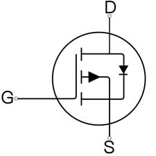
In a specific implementation, a low-power MOSFET Q1 for signal amplification is connected between the signal output terminal A of the PWM control chip and the primary of the pulse transformer Tl, the first output terminal of the secondary of the pulse transformer is connected to the gate of the first MOSFET Q4 via the diode D1 and the driving resistor Rl, the second output terminal of the secondary of the pulse transformer is connected to the gate of the second MOSFET Q5 via the diode D2 and the driving resistor R2, and the first output terminal of the secondary of the pulse transformer is also connected to the first drain triode Q2, and the second drain triode Q3 is also connected to the second drain triode Q3. MOSFET Q5, the first output terminal of the pulse transformer secondary is also connected to a first drain transistor Q2, and the second output terminal of the pulse transformer secondary is also connected to a second drain transistor Q3.
The gate of the first MOSFET Q4 is connected to a drain resistor R3, and the gate of the second MOSFET Q5 is connected to a drain resistor R4. the primary of the pulse transformer Tl is also connected to an energy storage and release circuit, and the energy storage and release circuit includes a resistor R5, a capacitor Cl, and a diode D3, and the resistor R5 and the capacitor Cl are connected in parallel, and the aforementioned parallel circuit is connected in series with the diode D3. the PWM signal output from the PWM control chip is connected to the low-power MOSFET Q2, and the low-power MOSFET Q2 is connected to the secondary of the pulse transformer. is amplified by the low-power MOSFET Ql and output to the primary of the pulse transformer Tl. When the PWM signal is high, the first output terminal and the second output terminal of the secondary of the pulse transformer Tl output high level signals to drive the first MOSFET Q4 and the second MOSFET Q5 to conduct.
When the PWM signal is low, the first output and the second output of the pulse transformer Tl secondary output low level signals, the first drain transistor Q2 and the second drain transistor Q3 conduction, the first MOSFETQ4 gate source capacitance through the drain resistor R3, the first drain transistor Q2 for discharge, the second MOSFETQ5 gate source capacitance through the drain resistor R4, the second drain transistor Q3 for discharge, the second MOSFETQ5 gate source capacitance through the drain resistor R4, the second drain transistor Q3 for discharge, the second MOSFETQ5 gate source capacitance through the drain resistor R4, the second drain transistor Q3 for discharge. The second MOSFETQ5 gate source capacitance is discharged through the drain resistor R4 and the second drain transistor Q3, so that the first MOSFET Q4 and the second MOSFET Q5 can be turned off faster and the power loss can be reduced.
When the PWM signal is low, the stored energy release circuit composed of resistor R5, capacitor Cl and diode D3 releases the stored energy in the pulse transformer when the PWM is high, ensuring that the gate source of the first MOSFET Q4 and the second MOSFET Q5 is extremely low, which serves the purpose of anti-interference. Diode Dl and diode D2 conduct the output current unidirectionally, thus ensuring the quality of the PWM waveform, and at the same time, it also plays the role of anti-interference to a certain extent.
-

Understanding the 4407A MOSFET: Your Friendly G...
-
MOSFET Package Switching Tube Selection and Cir...
-

Detailed explanation of the working principle d...
-
About the working principle of power MOSFET
-

What Are the Advantages of Power MOSFETs?
-

Did you know about the evolution of MOSFET?
-

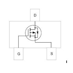
What do the three pins G, S, and D of the packa...
-

Olukey: Let’s talk about the role of MOSFET in ...
-

MOSFET Selection | N-Channel MOSFET Constructio...
-

The difference between N-channel MOSFET and P-c...
-
What are the four regions of a MOSFET?
-

Take a look at MOSFETs
-

How to prevent MOSFET failure
-

Do you know about depletion MOSFETs?
-

How to select the most suitable driver circuit ...
-
How to choose the right package MOSFET?


