


As one of the most basic devices in the semiconductor field, MOSFET is widely used in both IC design and board-level circuit applications. So how much do you know about the various parameters of MOSFET? As a specialist in medium and low voltage MOSFETs, Olukey will explain to you in detail the various parameters of MOSFETs!
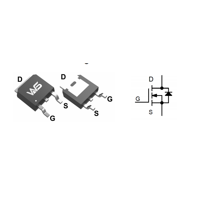
VDSS maximum drain-source withstand voltage
The drain-source voltage when the flowing drain current reaches a specific value (surges sharply) under a specific temperature and gate-source short circuit. The drain-source voltage in this case is also called avalanche breakdown voltage. VDSS has a positive temperature coefficient. At -50°C, VDSS is approximately 90% of that at 25°C. Due to the allowance usually left in normal production, the avalanche breakdown voltage of MOSFET is always greater than the nominal rated voltage.
Olukey’s warm reminder: In order to ensure product reliability, under the worst working conditions, it is recommended that the working voltage should not exceed 80~90% of the rated value.
VGSS maximum gate-source withstand voltage
It refers to the VGS value when the reverse current between gate and source begins to increase sharply. Exceeding this voltage value will cause dielectric breakdown of the gate oxide layer, which is a destructive and irreversible breakdown.
ID maximum drain-source current
It refers to the maximum current allowed to pass between the drain and the source when the field effect transistor is operating normally. The operating current of the MOSFET should not exceed ID. This parameter will derate as junction temperature increases.
IDM maximum pulse drain-source current
Reflects the level of pulse current that the device can handle. This parameter will decrease as the junction temperature increases. If this parameter is too small, the system may be at risk of being broken down by current during OCP testing.
PD maximum power dissipation
It refers to the maximum drain-source power dissipation allowed without deteriorating the performance of the field effect transistor. When used, the actual power consumption of the field effect transistor should be less than that of the PDSM and leave a certain margin. This parameter generally derates as junction temperature increases.
TJ, TSTG operating temperature and storage environment temperature range
These two parameters calibrate the junction temperature range allowed by the device's operating and storage environment. This temperature range is set to meet the minimum operating life requirements of the device. If the device is ensured to operate within this temperature range, its working life will be greatly extended.
-
Large Package MOSFET Driver Circuit
-

The connection between MOSFETs and Field Effect...
-
What is the principle of operation of MOSFET?
-

MOSFET Operating Characteristics
-

Analysis of important causes of MOSFET heat gen...
-

Power MOSFET: The Versatile Powerhouse of Moder...
-

Which brand of MOSFET is good
-

Important Steps on MOSFET Selection
-
What parameters should I pay attention to when ...
-

How much do you know about the MOSFET symbol?
-

What are the main features of MOSFETs?
-

Olukey: Let’s talk about the role of MOSFET in ...
-

MOSFET 101: The Ultimate Beginner’s Guide...
-

How MOSFETs work
-

MOSFET type and construction
-

How to determine the high-power MOSFET is burne...


