


The choice of MOSFET is very important, a bad choice may affect the power use of the entire circuit, master the nuances of different MOSFET components and parameters in different switching circuits can help engineers to avoid a lot of problems, the following are some of the recommendations of Guanhua Weiye for the selection of MOSFETs.
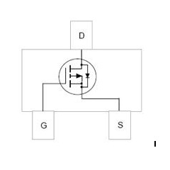
First, P-channel and N-channel
The first step is to determine the use of N-channel or P-channel MOSFETs. in power applications, when a MOSFET ground, and the load is connected to the trunk voltage, the MOSFET constitutes a low-voltage side switch. In low voltage side switching, N-channel MOSFETs are generally used, which is a consideration for the voltage required to turn off or turn on the device. When the MOSFET is connected to the bus and load ground, a high voltage side switch is used. P-channel MOSFETs are usually used, due to voltage drive considerations. To select the right components for the application, it is important to determine the voltage required to drive the device and how easy it is to implement in the design. The next step is to determine the required voltage rating, or the maximum voltage that the component can carry. The higher the voltage rating, the higher the cost of the device. In practice, the voltage rating should be greater than the trunk or bus voltage. This will provide enough protection so that the MOSFET will not fail. For MOSFET selection, it is important to determine the maximum voltage that can be withstood from drain to source, i.e., the maximum VDS, so it is important to know that the maximum voltage that the MOSFET can withstand varies with temperature. Designers need to test the voltage range over the entire operating temperature range. The rated voltage needs to have enough margin to cover this range to ensure that the circuit does not fail. In addition, other safety factors need to be considered induced voltage transients.
Second, determine the current rating
The current rating of the MOSFET depends on the circuit structure. The current rating is the maximum current that the load can withstand under all circumstances. Similar to the voltage case, the designer needs to make sure that the selected MOSFET is capable of carrying this rated current, even when the system generates a spike current. The two current scenarios to consider are continuous mode and pulse spikes. the MOSFET is in a steady state in continuous conduction mode, when current passes continuously through the device. Pulse spikes refer to a large number of surges (or spikes of current) flowing through the device, in which case, once the maximum current has been determined, it is simply a matter of directly selecting a device that can withstand this maximum current.
After selecting the rated current, the conduction loss is also calculated. In specific cases, MOSFET are not ideal components because of the electrical losses that occur during the conductive process, the so-called conduction losses. When "on", the MOSFET acts as a variable resistor, which is determined by the RDS(ON) of the device and changes significantly with temperature. The power loss of the device can be calculated from Iload2 x RDS(ON), and since the on-resistance varies with temperature, the power loss varies proportionally. The higher the voltage VGS applied to the MOSFET, the lower the RDS(ON); conversely, the higher the RDS(ON). For the system designer, this is where the tradeoffs come into play depending on the system voltage. For portable designs, lower voltages are easier (and more common), while for industrial designs, higher voltages can be used. Note that the RDS(ON) resistance rises slightly with current.

Technology has a tremendous impact on component characteristics, and some technologies tend to result in an increase in RDS(ON) when increasing the maximum VDS. For such technologies, an increase in wafer size is required if VDS and RDS(ON) are to be lowered, thus increasing the package size that goes with it and the corresponding development cost. There are a number of technologies in the industry that attempt to control the increase in wafer size, the most important of which are trench and charge balance technologies. In trench technology, a deep trench is embedded in the wafer, usually reserved for low voltages, to reduce the on-resistance RDS(ON).
III. Determine the heat dissipation requirements
The next step is to calculate the thermal requirements of the system. Two different scenarios need to be considered, the worst case and the real case. TPV recommends calculating the results for the worst-case scenario, as this calculation provides a greater margin of safety and ensures that the system will not fail.
IV. Switching Performance
Finally, the switching performance of the MOSFET. There are many parameters that affect the switching performance, the important ones are gate/drain, gate/source and drain/source capacitance. These capacitances form switching losses in the component due to the need to charge them every time they are switched. As a result, the switching speed of the MOSFET decreases and the efficiency of the device decreases. In order to calculate the total losses in the device during switching, the designer needs to calculate the losses during turn-on (Eon) and the losses during turn-off (Eoff). This can be expressed by the following equation: Psw = (Eon + Eoff) x switching frequency. And gate charge (Qgd) has the greatest impact on switching performance.
-

Do you know what an N-channel MOSFET is?
-
MOSFET overview
-

How to Determine nMOSFETs and pMOSFETs
-

How much do you know about MOSFET parameters? O...
-
What is the role of small voltage MOSFETs?
-
MOSFET Selection Points
-
MOSFET Package Switching Tube Selection and Cir...
-

What Are the Advantages of Power MOSFETs?
-

Characteristics of Enhanced MOSFETs
-
How to choose a MOSFET?
-

What is PMOSFET, do you know?
-
The connection between MOSFETs and Field Effect...
-

MOSFET Selection | N-Channel MOSFET Constructio...
-

Detailed explanation of the working principle d...
-

The three pins of a MOSFET, how can I tell them...
-

What can I do to fix my MOSFET that is heating ...


