


Power MOSFET is also divided into junction type and insulated gate type, but usually mainly refers to the insulated gate type MOSFET (Metal Oxide Semiconductor FET), referred to as power MOSFET (Power MOSFET). Junction type power field effect transistor is generally called electrostatic induction transistor (Static Induction Transistor - SIT). It is characterized by the gate voltage to control the drain current, drive circuit is simple, requires little drive power, fast switching speed, high operating frequency, thermal stability is better than the GTR, but its current capacity is small, low voltage, generally only applies to power not more than 10kW of power electronic devices.
1. Power MOSFET structure and operating principle
Power MOSFET types: according to the conductive channel can be divided into P-channel and N-channel. According to the gate voltage amplitude can be divided into; depletion type; when the gate voltage is zero when the drain-source pole between the existence of a conducting channel, enhanced; for N (P) channel device, the gate voltage is greater than (less than) zero before the existence of a conducting channel, the power MOSFET is mainly N-channel enhanced.
1.1 Power MOSFET structure
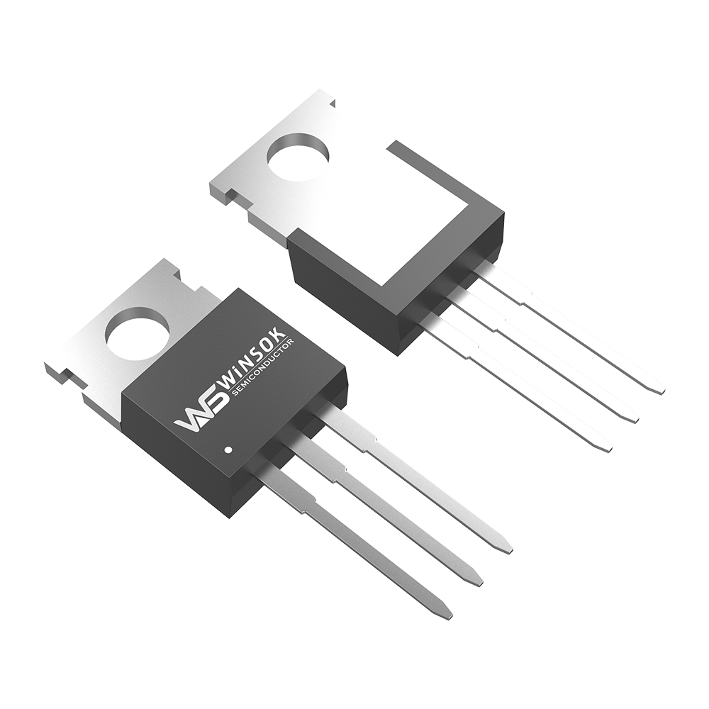
Power MOSFET internal structure and electrical symbols; its conduction only one polarity carriers (polys) involved in the conductive, is a unipolar transistor. Conducting mechanism is the same as the low-power MOSFET, but the structure has a big difference, the low-power MOSFET is a horizontal conductive device, the power MOSFET most of the vertical conductive structure, also known as the VMOSFET (Vertical MOSFET), which greatly improves the MOSFET device voltage and current withstand capability.
According to the differences in the vertical conductive structure, but also divided into the use of V-shaped groove to achieve vertical conductivity of the VVMOSFET and has a vertical conductive double-diffused MOSFET structure of the VDMOSFET (Vertical Double-diffused MOSFET), this paper is mainly discussed as an example of VDMOS devices.
Power MOSFETs for multiple integrated structure, such as International Rectifier (International Rectifier) HEXFET using a hexagonal unit; Siemens (Siemens) SIPMOSFET using a square unit; Motorola (Motorola) TMOS using a rectangular unit by the "Pin" shape arrangement.
1.2 Power MOSFET principle of operation
Cut-off: between the drain-source poles plus positive power supply, the gate-source poles between the voltage is zero. p base region and N drift region formed between the PN junction J1 reverse bias, no current flow between the drain-source poles.
Conductivity: With a positive voltage UGS applied between the gate-source terminals, the gate is insulated, so no gate current flows. However, the positive voltage of the gate will push away the holes in the P-region below it, and attract the oligons-electrons in the P-region to the surface of the P-region below the gate when the UGS is greater than the UT (turn-on voltage or threshold voltage), the concentration of electrons on the surface of the P-region under the gate will be more than the concentration of holes, so that the P-type semiconductor inverted into an N-type and become an inverted layer, and the inverted layer forms an N-channel and makes the PN junction J1 disappears, drain and source conductive.
1.3 Basic Characteristics of Power MOSFETs
1.3.1 Static Characteristics.
The relationship between the drain current ID and the voltage UGS between the gate source is called the transfer characteristic of the MOSFET, ID is larger, the relationship between ID and UGS is approximately linear, and the slope of the curve is defined as the transconductance Gfs.
The drain volt-ampere characteristics (output characteristics) of the MOSFET: cutoff region (corresponding to the cutoff region of the GTR); saturation region (corresponding to the amplification region of the GTR); non-saturation region (corresponding to the saturation region of the GTR). The power MOSFET operates in the switching state, i.e., it switches back and forth between the cutoff region and the non-saturation region. The power MOSFET has a parasitic diode between the drain-source terminals, and the device conducts when a reverse voltage is applied between the drain-source terminals. The on-state resistance of the power MOSFET has a positive temperature coefficient, which is favorable for equalizing the current when the devices are connected in parallel.
1.3.2 Dynamic Characterization;
its test circuit and switching process waveforms.
The turn-on process; turn-on delay time td(on) - the time period between the moment of up front and the moment when uGS = UT and iD starts to appear; rise time tr- the time period when uGS rises from uT to the gate voltage UGSP at which the MOSFET enters the non-saturated region; the steady state value of iD is determined by the drain supply voltage, UE, and the drain The magnitude of UGSP is related to the steady state value of iD. After UGS reaches UGSP, it continues to rise under the action of up until it reaches steady state, but iD is unchanged. Turn-on time ton-Sum of turn-on delay time and rise time.
Off delay time td(off) -The time period when iD starts to decrease to zero from the time up falls to zero, Cin is discharged through Rs and RG, and uGS falls to UGSP according to an exponential curve.
Falling time tf- The time period from when uGS continues to fall from UGSP and iD decreases until the channel disappears at uGS < UT and ID falls to zero. Turn-off time toff- The sum of the turn-off delay time and the fall time.
1.3.3 MOSFET switching speed.
MOSFET switching speed and Cin charging and discharging has a great relationship, the user can not reduce Cin, but can reduce the driving circuit internal resistance Rs to reduce the time constant, to speed up the switching speed, MOSFET only rely on the polytronic conductivity, there is no oligotronic storage effect, and thus the shutdown process is very rapid, the switching time of 10-100ns, the operating frequency can be up to 100kHz or more, is the highest of the main power electronic devices.
Field-controlled devices require almost no input current at rest. However, during the switching process, the input capacitor needs to be charged and discharged, which still requires a certain amount of driving power. The higher the switching frequency, the greater the drive power required.
1.4 Dynamic performance improvement
In addition to the device application to consider the device voltage, current, frequency, but also must master in the application of how to protect the device, not to make the device in the transient changes in the damage. Of course the thyristor is a combination of two bipolar transistors, coupled with a large capacitance due to the large area, so its dv/dt capability is more vulnerable. For di/dt it also has an extended conduction region problem, so it also imposes quite severe limitations.
The case of the power MOSFET is quite different. Its dv/dt and di/dt capability is often estimated in terms of capability per nanosecond (rather than per microsecond). But despite this, it has dynamic performance limitations. These can be understood in terms of the basic structure of a power MOSFET.
The structure of a power MOSFET and its corresponding equivalent circuit. In addition to the capacitance in almost every part of the device, it must be considered that the MOSFET has a diode connected in parallel. From a certain point of view, there is also a parasitic transistor. (Just as an IGBT also has a parasitic thyristor). These are important factors in the study of the dynamic behavior of MOSFETs.
First of all the intrinsic diode attached to the MOSFET structure has some avalanche capability. This is usually expressed in terms of single avalanche capability and repetitive avalanche capability. When the reverse di/dt is large, the diode is subjected to a very fast pulse spike, which has the potential to enter the avalanche region and potentially damage the device once its avalanche capability is exceeded. As with any PN junction diode, scrutinizing its dynamic characteristics is quite complex. They are very different from the simple concept of a PN junction conducting in the forward direction and blocking in the reverse direction. When the current drops rapidly, the diode loses its reverse blocking capability for a period of time known as the reverse recovery time. there is also a period of time when the PN junction is required to conduct rapidly and does not show a very low resistance. Once there is forward injection into the diode in a power MOSFET, the minority carriers injected also add to the complexity of the MOSFET as a multitronic device.

Transient conditions are closely related to line conditions, and this aspect should be given sufficient attention in the application. It is important to have an in-depth knowledge of the device in order to facilitate the understanding and analysis of the corresponding problems.
-

WINSOK|China e-Hotspot Solution Innovation Summ...
-
Large Package MOSFET Driver Circuit
-

The role of MOSFETs in circuits
-
How to choose the right package MOSFET?
-

MOSFET conduction characteristics
-
Understand MOSFET in onearticle
-

What are the main features of MOSFETs?
-

Do you know the definition of MOSFET?
-

Briefly talk about the production method of a h...
-

How MOSFETs work
-

Production method of high power MOSFET driving ...
-

How to correctly select small voltage MOSFETs
-

What is PMOSFET, do you know?
-
Main parameters of MOSFETs and comparison with ...
-

The Difference Between a Body Diode and MOSFET
-

Parallel Theory of MOSFETs and Transistors


