Quick Overview: MOSFETs can fail due to various electrical, thermal, and mechanical stresses. Understanding these failure modes is crucial for designing reliable power electronics systems. This comprehensive guide explores common failure mechanisms and prevention strategies.
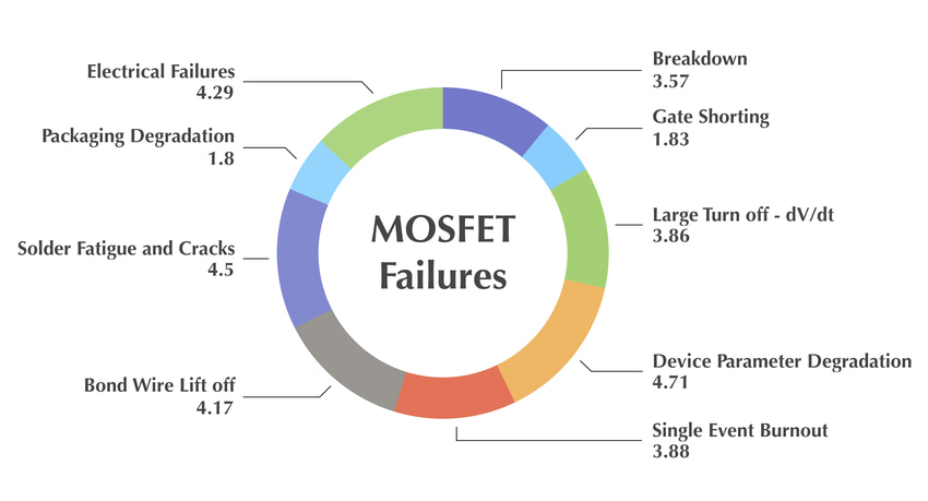 Common MOSFET Failure Modes and Their Root Causes
1. Voltage-Related Failures
- Gate oxide breakdown
- Avalanche breakdown
- Punch-through
- Static discharge damage
2. Thermal-Related Failures
- Secondary breakdown
- Thermal runaway
- Package delamination
- Bond wire lift-off
| Failure Mode | Primary Causes | Warning Signs | Prevention Methods |
|---|---|---|---|
| Gate Oxide Breakdown | Excessive VGS, ESD events | Increased gate leakage | Gate voltage protection, ESD measures |
| Thermal Runaway | Excessive power dissipation | Rising temperature, reduced switching speed | Proper thermal design, derating |
| Avalanche Breakdown | Voltage spikes, unclamped inductive switching | Drain-source short circuit | Snubber circuits, voltage clamps |
Winsok’s Robust MOSFET Solutions
Our latest generation of MOSFETs features advanced protection mechanisms:
- Enhanced SOA (Safe Operating Area)
- Improved thermal performance
- Built-in ESD protection
- Avalanche-rated designs
Detailed Analysis of Failure Mechanisms
Gate Oxide Breakdown
Critical Parameters:
- Maximum Gate-Source Voltage: ±20V typical
- Gate Oxide Thickness: 50-100nm
- Breakdown Field Strength: ~10 MV/cm
Prevention Measures:
- Implement gate voltage clamping
- Use series gate resistors
- Install TVS diodes
- Proper PCB layout practices
Thermal Management and Failure Prevention
| Package Type | Max Junction Temp | Recommended Derating | Cooling Solution |
|---|---|---|---|
| TO-220 | 175°C | 25% | Heatsink + Fan |
| D2PAK | 175°C | 30% | Large Copper Area + Optional Heatsink |
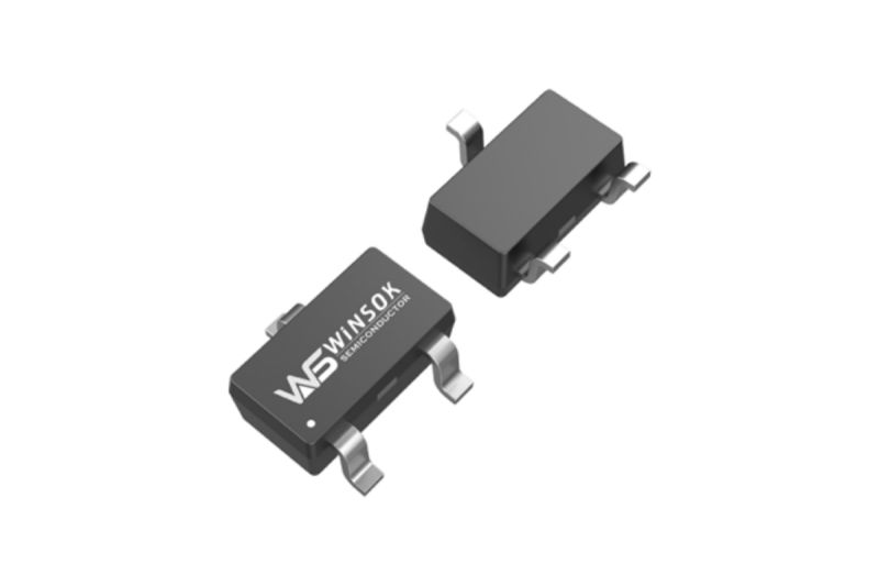
| SOT-23 | 150°C | 40% | PCB Copper Pour |
Essential Design Tips for MOSFET Reliability
PCB Layout
- Minimize gate loop area
- Separate power and signal grounds
- Use Kelvin source connection
- Optimize thermal vias placement
Circuit Protection
- Implement soft-start circuits
- Use appropriate snubbers
- Add reverse voltage protection
- Monitor device temperature
Diagnostic and Testing Procedures
Basic MOSFET Testing Protocol
- Static Parameters Testing
- Gate threshold voltage (VGS(th))
- Drain-source on-resistance (RDS(on))
- Gate leakage current (IGSS)
- Dynamic Testing
- Switching times (ton, toff)
- Gate charge characteristics
- Output capacitance
Winsok’s Reliability Enhancement Services
- Comprehensive application review
- Thermal analysis and optimization
- Reliability testing and validation
- Failure analysis laboratory support
Reliability Statistics and Lifetime Analysis
Key Reliability Metrics
FIT Rate (Failures In Time)
Number of failures per billion device-hours
Based on Winsok’s latest MOSFET series under nominal conditions
MTTF (Mean Time To Failure)
Expected lifetime under specified conditions
At TJ = 125°C, nominal voltage
Survival Rate
Percentage of devices surviving beyond warranty period
At 5 years of continuous operation
Lifetime Derating Factors
| Operating Condition | Derating Factor | Impact on Lifetime |
|---|---|---|
| Temperature (per 10°C above 25°C) | 0.5x | 50% reduction |
| Voltage Stress (95% of max rating) | 0.7x | 30% reduction |
| Switching Frequency (2x nominal) | 0.8x | 20% reduction |
| Humidity (85% RH) | 0.9x | 10% reduction |
Lifetime Probability Distribution
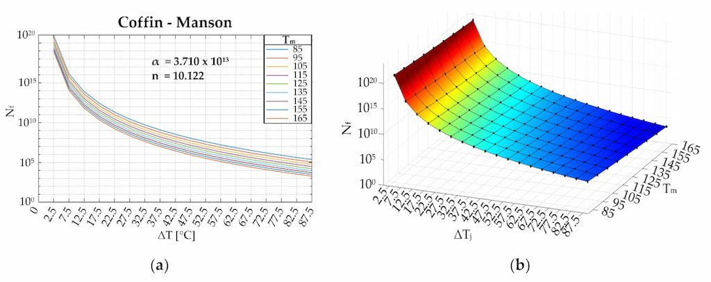
Weibull distribution of MOSFET lifetime showing early failures, random failures, and wear-out period
Environmental Stress Factors
Temperature Cycling
Impact on lifetime reduction
Power Cycling
Impact on lifetime reduction
Mechanical Stress
Impact on lifetime reduction
Accelerated Life Testing Results
| Test Type | Conditions | Duration | Failure Rate |
|---|---|---|---|
| HTOL (High Temperature Operating Life) | 150°C, Max VDS | 1000 hours | < 0.1% |
| THB (Temperature Humidity Bias) | 85°C/85% RH | 1000 hours | < 0.2% |
| TC (Temperature Cycling) | -55°C to +150°C | 1000 cycles | < 0.3% |


