


First of all, the MOSFET type and structure, MOSFET is a FET (another is JFET), can be manufactured into enhanced or depletion type, P-channel or N-channel a total of four types, but the actual application of only enhanced N-channel MOSFETs and enhanced P-channel MOSFETs, so usually referred to as the NMOS or PMOS refers to these two kinds. For these two types of enhanced MOSFETs, the more commonly used is NMOS, the reason is that the on-resistance is small, and easy to manufacture. Therefore, NMOS is generally used in switching power supply and motor drive applications.
In the following introduction, most of the cases are dominated by NMOS. parasitic capacitance exists between the three pins of the MOSFET, a feature that is not needed but arises due to manufacturing process limitations. The presence of parasitic capacitance makes it a bit tricky to design or select a driver circuit. There is a parasitic diode between the drain and the source. This is called the body diode and is important in driving inductive loads such as motors. By the way, the body diode is only present in individual MOSFETs and is usually not present inside an IC chip.

MOSFET switching tube loss, whether it is NMOS or PMOS, after the conduction of the on-resistance exists, so that the current will consume energy in this resistance, this part of the consumed energy is called conduction loss. Selection of MOSFETs with low on-resistance will reduce the on-resistance loss. Nowadays, the on-resistance of low-power MOSFETs is generally around tens of milliohms, and a few milliohms are also available.MOSFETs must not be completed in an instant when they are on and off.There is a process of decreasing the voltage at the two ends of the MOSFET, and there is a process of increasing the current flowing through it.During this period of time, the loss of MOSFETs is the product of the voltage and the current, which is called the switching loss. Usually the switching loss is much larger than the conduction loss, and the faster the switching frequency, the larger the loss. The product of voltage and current at the instant of conduction is very large, resulting in large losses. Shortening the switching time reduces the loss at each conduction; reducing the switching frequency reduces the number of switches per unit time. Both of these approaches reduce the switching losses.
Compared to bipolar transistors, it is generally believed that no current is required to make a MOSFET conduct, as long as the GS voltage is above a certain value. This is easy to do, however, we also need speed. As you can see in the structure of the MOSFET, there is a parasitic capacitance between GS, GD, and the driving of the MOSFET is, in effect, the charging and discharging of the capacitance. Charging the capacitor requires a current, because charging the capacitor instantly can be seen as a short circuit, so the instantaneous current will be higher. The first thing to note when selecting/designing a MOSFET driver is the size of the instantaneous short-circuit current that can be provided.
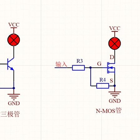
The second thing to note is that, generally used in high-end drive NMOS, the on-time gate voltage needs to be greater than the source voltage. High-end drive MOSFET on the source voltage and drain voltage (VCC) the same, so then the gate voltage than the VCC 4V or 10V. if in the same system, to get a larger voltage than the VCC, we need to specialize in the boost circuit. Many motor drivers have integrated charge pumps, it is important to note that you should choose the appropriate external capacitance to get enough short-circuit current to drive the MOSFET. 4V or 10V is the commonly used MOSFET on voltage, the design of course, you need to have a certain margin. The higher the voltage, the faster the on-state speed and the lower the on-state resistance. Now there are also smaller on-state voltage MOSFETs used in different fields, but in the 12V automotive electronics system, generally 4V on-state is enough.MOSFETs most notable feature is the switching characteristics of the good, so it is widely used in the need for electronic switching circuits, such as switching power supply and motor drive, but also lighting dimming. Conducting means acting as a switch, which is equivalent to a switch closure.NMOS characteristics, Vgs greater than a certain value will conduct, suitable for use in the case when the source is grounded (low-end drive), as long as the gate voltage of 4V or 10V.PMOS characteristics, Vgs less than a certain value will conduct, suitable for use in the case when the source is connected to the VCC (high-end drive). However, although PMOS can be easily used as a high end driver, NMOS is usually used in high end drivers due to the large on-resistance, high price, and few replacement types.
Now the MOSFET drive low-voltage applications, when the use of 5V power supply, this time if you use the traditional totem pole structure, due to the transistor be about 0.7V voltage drop, resulting in the actual final added to the gate on the voltage is only 4.3 V. At this time, we choose the nominal gate voltage of 4.5V of the MOSFET on the existence of certain risks. The same problem occurs in the use of 3V or other low-voltage power supply occasions. Dual voltage is used in some control circuits where the logic section uses a typical 5V or 3.3V digital voltage and the power section uses 12V or even higher. The two voltages are connected using a common ground. This puts a requirement to use a circuit that allows the low voltage side to effectively control the MOSFET on the high voltage side, while the MOSFET on the high voltage side will face the same problems mentioned in 1 and 2. In all three cases, the totem pole structure cannot meet the output requirements, and many off-the-shelf MOSFET driver ICs do not seem to include a gate voltage limiting structure. The input voltage is not a fixed value, it varies with time or other factors. This variation causes the drive voltage provided to the MOSFET by the PWM circuit to be unstable. In order to make the MOSFET safe from high gate voltages, many MOSFETs have built-in voltage regulators to forcefully limit the amplitude of the gate voltage.
In this case, when the drive voltage provided exceeds the voltage of the regulator, it will cause a large static power consumption At the same time, if you simply use the principle of resistor voltage divider to reduce the gate voltage, there will be a relatively high input voltage, the MOSFET works well, while the input voltage is reduced when the gate voltage is insufficient to cause insufficiently complete conduction, thus increasing power consumption.
Relatively common circuit here only for the NMOS driver circuit to do a simple analysis: Vl and Vh are the low-end and high-end power supply, respectively, the two voltages can be the same, but Vl should not exceed Vh. Q1 and Q2 form an inverted totem pole, used to achieve the isolation, and at the same time to ensure that the two driver tubes Q3 and Q4 will not be on at the same time. R2 and R3 provide the PWM voltage reference, and by changing this reference, you can make the circuit work well, and the gate voltage is not enough to cause a thorough conduction, thus increasing the power consumption. R2 and R3 provide the PWM voltage reference, by changing this reference, you can let the circuit work in the PWM signal waveform is relatively steep and straight position. Q3 and Q4 are used to provide the drive current, due to the on-time, Q3 and Q4 relative to the Vh and GND are only a minimum of a Vce voltage drop, this voltage drop is usually only 0.3V or so, much lower than 0.7V Vce R5 and R6 are feedback resistors for the gate voltage sampling, after sampling the voltage, the voltage of the gate is used as a feedback resistor to the gate voltage, and the voltage of the sample is used to the gate voltage. R5 and R6 are feedback resistors used to sample the gate voltage, which is then passed through Q5 to create a strong negative feedback on the bases of Q1 and Q2, thus limiting the gate voltage to a finite value. This value can be adjusted by R5 and R6. Finally, R1 provides the limitation of the base current to Q3 and Q4, and R4 provides the limitation of the gate current to the MOSFETs, which is the limitation of the Ice of Q3Q4. An acceleration capacitor can be connected in parallel above R4 if necessary.
When designing portable devices and wireless products, improving product performance and extending battery operating time are two issues designers need to face.DC-DC converters have the advantages of high efficiency, high output current and low quiescent current, which are very suitable for powering portable devices.
DC-DC converters have the advantages of high efficiency, high output current and low quiescent current, which are very suitable for powering portable devices. Currently, the main trends in the development of DC-DC converter design technology include: high-frequency technology: with the increase in switching frequency, the size of the switching converter is also reduced, the power density has been significantly increased, and the dynamic response has been improved. Small
Power DC-DC converter switching frequency will rise to the megahertz level. Low output voltage technology: With the continuous development of semiconductor manufacturing technology, microprocessors and portable electronic equipment operating voltage is getting lower and lower, which requires future DC-DC converter can provide low output voltage to adapt to the microprocessor and portable electronic equipment, which requires future DC-DC converter can provide low output voltage to adapt to the microprocessor.
Enough to provide low output voltage to adapt to microprocessors and portable electronic equipment. These technological developments put forward higher requirements for the design of power supply chip circuits. First of all, with the increasing switching frequency, the performance of the switching components is put forward
High requirements for the performance of the switching element, and must have the corresponding switching element drive circuit to ensure that the switching element in the switching frequency up to the megahertz level of normal operation. Secondly, for battery-powered portable electronic devices, the circuit's operating voltage is low (in the case of lithium batteries, for example).
Lithium batteries, for example, the operating voltage of 2.5 ~ 3.6V), so the power supply chip for the lower voltage.
MOSFET has a very low on-resistance, low energy consumption, in the current popular high-efficiency DC-DC chip more MOSFET as a power switch. However, due to the large parasitic capacitance of MOSFETs. This puts higher requirements on the design of switching tube driver circuits for designing high operating frequency DC-DC converters. There are various CMOS, BiCMOS logic circuits using bootstrap boost structure and driver circuits as large capacitive loads in low voltage ULSI design. These circuits are able to work properly under the conditions of less than 1V voltage supply, and can work under the conditions of load capacitance 1 ~ 2pF frequency can reach tens of megabits or even hundreds of megahertz. In this paper, the bootstrap boost circuit is used to design a large load capacitance drive capability, suitable for low-voltage, high switching frequency boost DC-DC converter drive circuit. Low-end voltage and PWM to drive high-end MOSFETs. small amplitude PWM signal to drive high gate voltage requirements of MOSFETs.


-

About MOSFET driver
-

Do you know the MOSFET driver circuit?
-

Differences Between IGBT and MOSFET
-

How MOSFETs work
-
Explanation of each parameter of power MOSFETs
-

How much do you know about MOSFET parameters? O...
-

Is the MOSFET fully or half controlled?
-

MOSFET substitution principle and good and bad ...
-
What are the four regions of a MOSFET?
-

Semiconductor Market Status of Electronic Infor...
-
What are the differences between MOSFETs and Tr...
-

Flow of MOSFET testing
-

Power MOSFET Package Types Guide
-

Understanding Cascode Amplifier MOSFETs: The Ul...
-

Important Steps on MOSFET Selection
-

The role of MOSFETs in circuits


