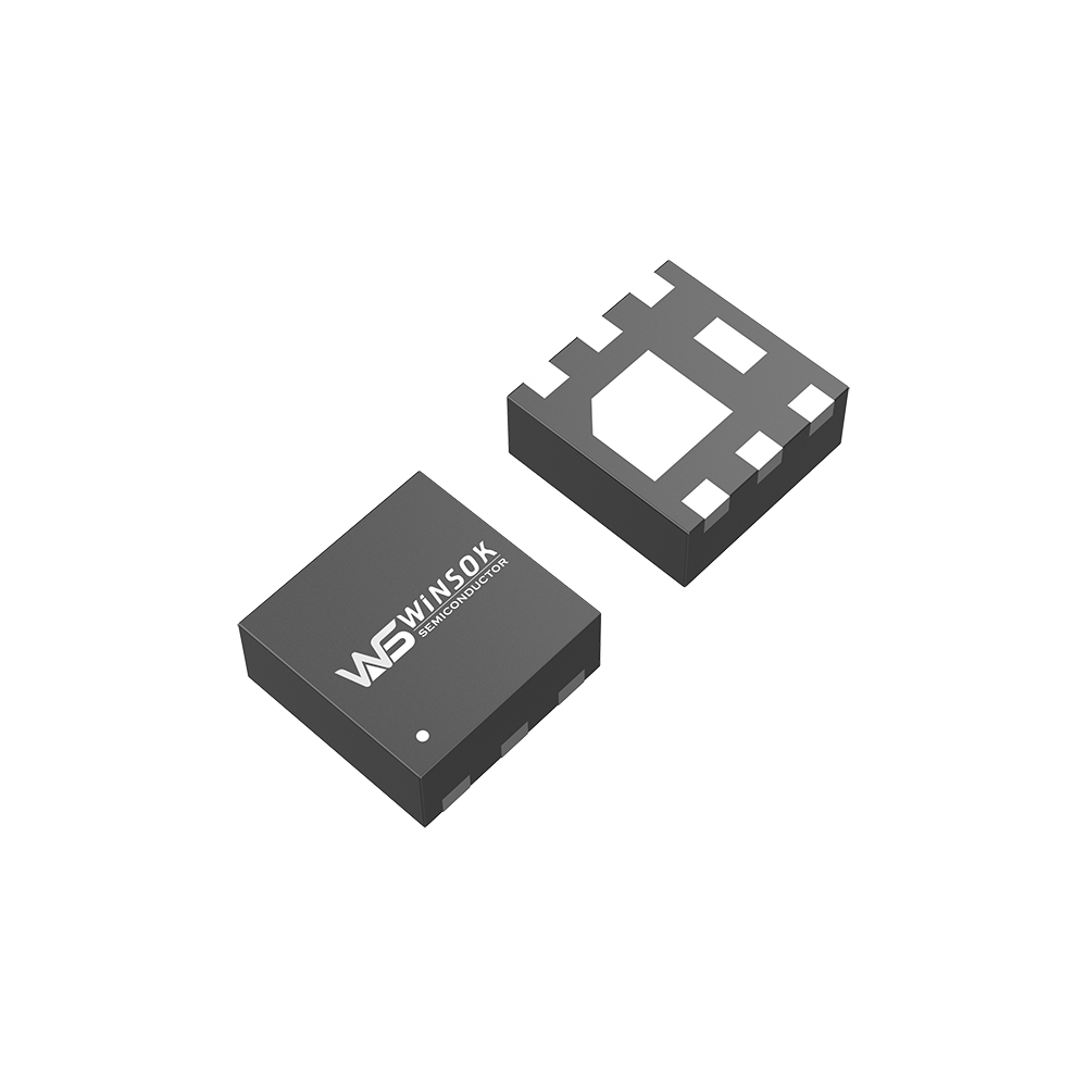
Small voltage MOSFET selection is a very important part of the MOSFET selection is not good may affect the efficiency and cost of the entire circuit, but also will bring a lot of trouble to the engineers, that how to correctly select the MOSFET?
Choosing N-channel or P-channel The first step in selecting the correct device for a design is to decide whether to use an N-channel or P-channel MOSFET In a typical power application, a MOSFET constitutes a low-voltage side switch when the MOSFET is grounded and the load is connected to the trunk voltage. In a low voltage side switch, an N-channel MOSFET should be used due to the consideration of the voltage required to turn off or turn on the device.
When the MOSFET is connected to the bus and the load is grounded, the high voltage side switch is to be used. P-channel MOSFETs are usually used in this topology, again for voltage drive considerations. Determine the current rating. Select the current rating of the MOSFET. Depending on the circuit structure, this current rating should be the maximum current that the load can withstand under all circumstances.
Similar to the case of voltage, the designer must ensure that the selected MOSFET can withstand this current rating, even when the system is generating spike currents. The two current cases to consider are continuous mode and pulse spikes. In continuous conduction mode, the MOSFET is in steady state, when current passes continuously through the device.
Pulse spikes are when there are large surges (or spikes of current) flowing through the device. Once the maximum current under these conditions has been determined, it is simply a matter of directly selecting a device that can withstand this maximum current. Determining Thermal Requirements Selecting a MOSFET also requires calculating the thermal requirements of the system. The designer must consider two different scenarios, the worst case and the true case. It is recommended that the worst-case calculation be used because it provides a greater margin of safety and ensures that the system will not fail. There are also some measurements to be aware of on the MOSFET data sheet; such as the thermal resistance between the semiconductor junction of the package device and the environment, and the maximum junction temperature. Deciding on switching performance, the final step in selecting a MOSFET is to decide on the switching performance of the MOSFET.
There are many parameters that affect switching performance, but the most important are gate/drain, gate/source, and drain/source capacitance. These capacitances create switching losses in the device because they have to be charged during each switching. the switching speed of the MOSFET is therefore reduced and the efficiency of the device decreases. To calculate the total device losses during switching, the designer must calculate the turn-on losses (Eon) and the turn-off losses.
When the value of vGS is small, the ability to absorb electrons is not strong, leakage - source between the still no conductive channel presents, vGS increase, absorbed into the P substrate outer surface layer of electrons on the increase, when the vGS reaches a certain value, these electrons in the gate near the P substrate appearance constitutes a thin layer of N-type, and with the two N + zone connected When vGS reaches a certain value, these electrons in the gate near the P substrate appearance will constitute a N-type thin layer, and connected to the two N + region, in the drain - source constitute N-type conductive channel, its conductive type and the opposite of the P substrate, constituting the anti-type layer. vGS is larger, the role of the semiconductor appearance of the stronger the electric field, the absorption of electrons to the exterior of the P substrate, the more the conductive channel is thicker, the lower the channel resistance. That is, N-channel MOSFET in vGS < VT, can not constitute a conductive channel, the tube is in the cutoff state. As long as when vGS ≥ VT, only when the channel composition. After the channel is constituted, a drain current is generated by adding a forward voltage vDS between the drain - source.
But Vgs continues to increase, let's say IRFPS40N60KVgs = 100V when Vds = 0 and Vds = 400V, two conditions, the tube function to bring what effect, if burned, the cause and the internal mechanism of the process is how to Vgs increase will reduce Rds (on) reduce switching losses, but at the same time will increase the Qg, so that the turn-on loss becomes larger, affecting the efficiency of the MOSFET GS voltage by Vgg to Cgs charging and rise, arrived at the maintenance voltage Vth, MOSFET start conductive; MOSFET DS current increase, Millier capacitance in the interval due to the discharge of DS capacitance and discharge, GS capacitance charging does not have much impact; Qg = Cgs * Vgs, but the charge will continue to build up.
The DS voltage of the MOSFET drops to the same voltage as Vgs, the Millier capacitance increases greatly, the external drive voltage stops charging the Millier capacitance, the voltage of the GS capacitance remains unchanged, the voltage on the Millier capacitance increases, while the voltage on the DS capacitance continues to decrease; the DS voltage of the MOSFET decreases to the voltage at saturated conduction, the Millier capacitance becomes smaller The DS voltage of the MOSFET drops to the voltage at saturation conduction, the Millier capacitance becomes smaller and is charged together with the GS capacitance by the external drive voltage, and the voltage on the GS capacitance rises; the voltage measurement channels are the domestic 3D01, 4D01, and Nissan's 3SK series.
G-pole (gate) determination: use the diode gear of the multimeter. If a foot and the other two feet between the positive and negative voltage drop are greater than 2V, that is, the display "1", this foot is the gate G. And then exchange the pen to measure the rest of the two feet, the voltage drop is small that time, the black pen is connected to the D-pole (drain), the red pen is connected to the S-pole (source).


