


"MOSFET" is the abbreviation of Metal Oxide Semicoductor Field Effect Transistor. It is a device made of three materials: metal, oxide (SiO2 or SiN) and semiconductor. MOSFET is one of the most basic devices in the semiconductor field. Whether it is in IC design or board-level circuit applications, it is very extensive. The main parameters of MOSFET include ID, IDM, VGSS, V(BR)DSS, RDS(on), VGS(th), etc. Do you know these? OLUKEY Company, as a winsok Taiwanese mid-to-high-end medium and low-voltage MOSFET agent service provider, has a core team with nearly 20 years of experience to explain to you in detail the various parameters of MOSFET!
Description of the meaning of MOSFET parameters
1. Extreme parameters:
ID: Maximum drain-source current. It refers to the maximum current allowed to pass between the drain and the source when the field effect transistor is operating normally. The operating current of the field effect transistor should not exceed ID. This parameter decreases as junction temperature increases.
IDM: Maximum pulsed drain-source current. This parameter will decrease as the junction temperature increases, reflecting an impact resistance and is also related to the pulse time. If this parameter is too small, the system may be at risk of being broken down by current during OCP testing.
PD: Maximum power dissipated. It refers to the maximum drain-source power dissipation allowed without deteriorating the performance of the field effect transistor. When used, the actual power consumption of the FET should be less than that of the PDSM and leave a certain margin. This parameter generally decreases as the junction temperature increases
VDSS: Maximum drain-source withstand voltage. The drain-source voltage when the flowing drain current reaches a specific value (surges sharply) under a specific temperature and gate-source short circuit. The drain-source voltage in this case is also called avalanche breakdown voltage. VDSS has a positive temperature coefficient. At -50°C, VDSS is approximately 90% of that at 25°C. Due to the allowance usually left in normal production, the avalanche breakdown voltage of MOSFET is always greater than the nominal rated voltage.
OLUKEY Warm Tips: To ensure product reliability, under the worst working conditions, it is recommended that the working voltage should not exceed 80~90% of the rated value.
VGSS: Maximum gate-source withstand voltage. It refers to the VGS value when the reverse current between gate and source begins to increase sharply. Exceeding this voltage value will cause dielectric breakdown of the gate oxide layer, which is a destructive and irreversible breakdown.
TJ: Maximum operating junction temperature. It is usually 150℃ or 175℃. Under the working conditions of device design, it is necessary to avoid exceeding this temperature and leave a certain margin.
TSTG: storage temperature range
These two parameters, TJ and TSTG, calibrate the junction temperature range allowed by the device's working and storage environment. This temperature range is set to meet the minimum operating life requirements of the device. If the device is ensured to operate within this temperature range, its working life will be greatly extended.
2. Static parameters
MOSFET test conditions are generally 2.5V, 4.5V, and 10V.
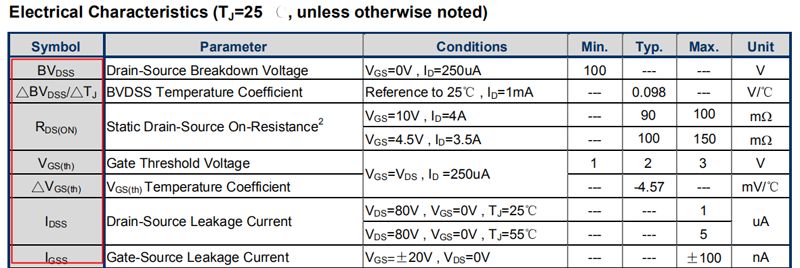
V(BR)DSS: Drain-source breakdown voltage. It refers to the maximum drain-source voltage that the field effect transistor can withstand when the gate-source voltage VGS is 0. This is a limiting parameter, and the operating voltage applied to the field effect transistor must be less than V(BR)DSS. It has positive temperature characteristics. Therefore, the value of this parameter under low temperature conditions should be taken as a safety consideration.
△V(BR)DSS/△Tj: Temperature coefficient of drain-source breakdown voltage, generally 0.1V/℃
RDS(on): Under certain conditions of VGS (usually 10V), junction temperature and drain current, the maximum resistance between drain and source when the MOSFET is turned on. It is a very important parameter that determines the power consumed when the MOSFET is turned on. This parameter generally increases as junction temperature increases. Therefore, the value of this parameter at the highest operating junction temperature should be used for calculation of loss and voltage drop.
VGS(th): turn-on voltage (threshold voltage). When the external gate control voltage VGS exceeds VGS(th), the surface inversion layers of the drain and source regions form a connected channel. In applications, the gate voltage when ID is equal to 1 mA under the drain short-circuit condition is often called the turn-on voltage. This parameter generally decreases as junction temperature increases
IDSS: saturated drain-source current, the drain-source current when the gate voltage VGS=0 and VDS is a certain value. Generally at the microamp level
IGSS: gate-source drive current or reverse current. Since the MOSFET input impedance is very large, IGSS is generally in the nanoamp level.
3. Dynamic parameters
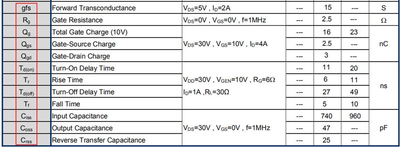
gfs: transconductance. It refers to the ratio of the change in drain output current to the change in gate-source voltage. It is a measure of the ability of gate-source voltage to control drain current. Please look at the chart for the transfer relationship between gfs and VGS.
Qg: Total gate charging capacity. MOSFET is a voltage-type driving device. The driving process is the establishment process of gate voltage. This is achieved by charging the capacitance between gate source and gate drain. This aspect will be discussed in detail below.
Qgs: Gate source charging capacity
Qgd: gate-to-drain charge (taking into account Miller effect). MOSFET is a voltage-type driving device. The driving process is the establishment process of gate voltage. This is achieved by charging the capacitance between gate source and gate drain.
Td(on): conduction delay time. The time from when the input voltage rises to 10% until VDS drops to 90% of its amplitude
Tr: rise time, the time for the output voltage VDS to drop from 90% to 10% of its amplitude
Td(off): Turn-off delay time, the time from when the input voltage drops to 90% to when VDS rises to 10% of its turn-off voltage
Tf: Fall time, the time for the output voltage VDS to rise from 10% to 90% of its amplitude
Ciss: Input capacitance, short-circuit the drain and source, and measure the capacitance between the gate and the source with an AC signal. Ciss= CGD + CGS (CDS short circuit). It has a direct impact on the turn-on and turn-off delays of the device.
Coss: Output capacitance, short-circuit the gate and source, and measure the capacitance between the drain and the source with an AC signal. Coss = CDS +CGD
Crss: Reverse transmission capacitance. With the source connected to ground, the measured capacitance between the drain and gate Crss=CGD. One of the important parameters for switches is the rise and fall time. Crss=CGD
The interelectrode capacitance and MOSFET induced capacitance of MOSFET are divided into input capacitance, output capacitance and feedback capacitance by most manufacturers. The values quoted are for a fixed drain-to-source voltage. These capacitances change as the drain-source voltage changes, and the value of the capacitance has a limited effect. The input capacitance value only gives an approximate indication of the charging required by the driver circuit, whereas the gate charging information is more useful. It indicates the amount of energy the gate must charge to reach a specific gate-to-source voltage.
4. Avalanche breakdown characteristic parameters
The avalanche breakdown characteristic parameter is an indicator of the MOSFET's ability to withstand overvoltage in the off state. If the voltage exceeds the drain-source limit voltage, the device will be in an avalanche state.
EAS: Single pulse avalanche breakdown energy. This is a limit parameter, indicating the maximum avalanche breakdown energy that the MOSFET can withstand.
IAR: avalanche current
EAR: Repeated Avalanche Breakdown Energy
5. In vivo diode parameters
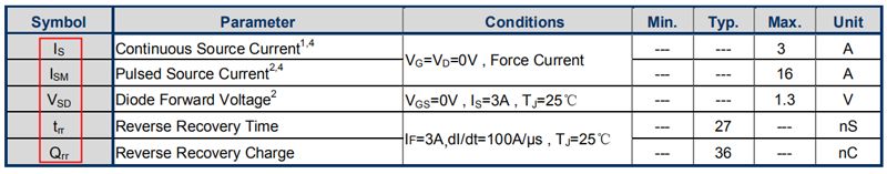
IS: Continuous maximum freewheeling current (from source)
ISM: pulse maximum freewheeling current (from source)
VSD: forward voltage drop
Trr: reverse recovery time
Qrr: Reverse charge recovery
Ton: Forward conduction time. (Basically negligible)
MOSFET turn-on time and turn-off time definition
During the application process, the following characteristics often need to be considered:
1. Positive temperature coefficient characteristics of V (BR) DSS. This characteristic, which is different from bipolar devices, makes them more reliable as normal operating temperatures increase. But you also need to pay attention to its reliability during low-temperature cold starts.
2. Negative temperature coefficient characteristics of V(GS)th. The gate threshold potential will decrease to a certain extent as the junction temperature increases. Some radiation will also reduce this threshold potential, possibly even below 0 potential. This feature requires engineers to pay attention to the interference and false triggering of MOSFETs in these situations, especially for MOSFET applications with low threshold potentials. Due to this characteristic, it is sometimes necessary to design the off-voltage potential of the gate driver to a negative value (referring to N-type, P-type and so on) to avoid interference and false triggering.
3.Positive temperature coefficient characteristics of VDSon/RDSo. The characteristic that VDSon/RDSon increases slightly as the junction temperature increases makes it possible to directly use MOSFETs in parallel. Bipolar devices are just the opposite in this regard, so their use in parallel becomes quite complicated. RDSon will also increase slightly as ID increases. This characteristic and the positive temperature characteristics of junction and surface RDSon enable MOSFET to avoid secondary breakdown like bipolar devices. However, it should be noted that the effect of this feature is quite limited. When used in parallel, push-pull or other applications, you cannot completely rely on the self-regulation of this feature. Some fundamental measures are still needed. This characteristic also explains that conduction losses become larger at high temperatures. Therefore, special attention should be paid to the selection of parameters when calculating losses.
4. The negative temperature coefficient characteristics of ID, understanding of MOSFET parameters and its main characteristics ID will decrease significantly as the junction temperature increases. This characteristic makes it often necessary to consider its ID parameters at high temperatures during design.
5. Negative temperature coefficient characteristics of avalanche capability IER/EAS. After the junction temperature increases, although the MOSFET will have a larger V(BR)DSS, it should be noted that the EAS will be significantly reduced. That is to say, its ability to withstand avalanches under high temperature conditions is much weaker than that at normal temperatures.
6. The conduction capability and reverse recovery performance of the parasitic diode in the MOSFET are no better than that of ordinary diodes. It is not expected to be used as the main current carrier in the loop in the design. Blocking diodes are often connected in series to invalidate the parasitic diodes in the body, and additional parallel diodes are used to form a circuit electrical carrier. However, it can be considered as a carrier in the case of short-term conduction or some small current requirements such as synchronous rectification.
7. The rapid rise of the drain potential may cause spurious-triggering of the gate drive, so this possibility needs to be considered in large dVDS/dt applications (high-frequency fast switching circuits).
Post time: Dec-13-2023


