The working principle of MOSFET is mainly based on its unique structural properties and electric field effects. The following is a detailed explanation of how MOSFETs work:
I. Basic structure of MOSFET
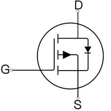
A MOSFET consists mainly of a gate (G), a source (S), a drain (D), and a substrate (B, sometimes connected to the source to form a three-terminal device). In N-channel enhancement MOSFETs, the substrate is usually a low-doped P-type silicon material on which two highly doped N-type regions are fabricated to serve as the source and drain, respectively. The surface of the P-type substrate is covered with a very thin oxide film (silicon dioxide) as an insulating layer, and an electrode is drawn as the gate. This structure makes the gate insulated from the P-type semiconductor substrate, the drain and the source, and is therefore also called an insulated-gate field effect tube.
II. Principle of operation
MOSFETs operate by using the gate source voltage (VGS) to control the drain current (ID). Specifically, when the applied positive gate source voltage, VGS, is greater than zero, an upper positive and lower negative electric field will appear on the oxide layer below the gate. This electric field attracts free electrons in the P-region, causing them to accumulate below the oxide layer, while repelling holes in the P-region. As VGS increases, the strength of the electric field increases and the concentration of attracted free electrons increases. When VGS reaches a certain threshold voltage (VT), the concentration of free electrons gathered in the region is large enough to form a new N-type region (N-channel), which acts like a bridge connecting the drain and source. At this point, if a certain driving voltage (VDS) exists between the drain and source, the drain current ID starts to flow.
III. Formation and change of conducting channel
The formation of the conducting channel is the key to the operation of the MOSFET. When VGS is greater than VT, the conducting channel is established and the drain current ID is affected by both VGS and VDS.VGS affects ID by controlling the width and shape of the conducting channel, while VDS affects ID directly as the driving voltage.It is important to note that if the conducting channel is not established (i.e., VGS is less than VT), then even if VDS is present, the drain current ID does not appear.
IV. Characteristics of MOSFETs
High input impedance:The input impedance of the MOSFET is very high, close to infinity, because there is an insulating layer between the gate and the source-drain region and only a weak gate current.
Low output impedance:MOSFETs are voltage-controlled devices in which the source-drain current can change with the input voltage, so their output impedance is small.
Constant flow:When operating in the saturation region, the current of the MOSFET is virtually unaffected by changes in the source-drain voltage, providing excellent constant current.
Good temperature stability:The MOSFETs have a wide operating temperature range from -55°C to about +150°C.
V. Applications and classifications
MOSFETs are widely used in digital circuits, analogue circuits, power circuits and other fields. According to the type of operation, MOSFETs can be classified into enhancement and depletion types; according to the type of conducting channel, they can be classified into N-channel and P-channel. These different types of MOSFETs have their own advantages in different application scenarios.
In summary, the working principle of MOSFET is to control the formation and change of the conducting channel through the gate source voltage, which in turn controls the flow of drain current. Its high input impedance, low output impedance, constant current and temperature stability make MOSFETs an important component in electronic circuits.


