
MOSFET is one of the most basic components in the semiconductor industry. In electronic circuits, MOSFET is generally used in power amplifier circuits or switching power supply circuits and is widely used. Below, OLUKEY will give you a detailed explanation of the working principle of MOSFET and analyze the internal structure of MOSFET.
What is MOSFET
MOSFET, Metal Oxide Semiconductor Filed Effect Transistor (MOSFET). It is a field effect transistor that can be widely used in analog circuits and digital circuits. According to the polarity difference of its "channel" (working carrier), it can be divided into two types: "N-type" and "P-type", which are often called NMOS and PMOS.
MOSFET working principle
MOSFET can be divided into enhancement type and depletion type according to the working mode. The enhancement type refers to the MOSFET when no bias voltage is applied and there is no conductive channel. The depletion type refers to the MOSFET when no bias voltage is applied. A conductive channel will appear.
In actual applications, there are only N-channel enhancement type and P-channel enhancement type MOSFETs. Since NMOSFETs have small on-state resistance and are easy to manufacture, NMOS is more common than PMOS in actual applications.
Enhancement mode MOSFET
There are two back-to-back PN junctions between the drain D and source S of the enhancement-mode MOSFET. When the gate-source voltage VGS=0, even if the drain-source voltage VDS is added, there is always a PN junction in a reverse-biased state, and there is no conductive channel between the drain and the source (no current flows). Therefore, the drain current ID=0 at this time.
At this time, if a forward voltage is added between the gate and the source. That is, VGS>0, then an electric field with the gate aligned with the P-type silicon substrate will be generated in the SiO2 insulating layer between the gate electrode and the silicon substrate. Because the oxide layer is insulating, the voltage VGS applied to the gate cannot produce current. A capacitor is generated on both sides of the oxide layer, and the VGS equivalent circuit charges this capacitor (capacitor). And generate an electric field, as VGS slowly rises, attracted by the positive voltage of the gate. A large number of electrons accumulate on the other side of this capacitor (capacitor) and create an N-type conductive channel from drain to source. When VGS exceeds the turn-on voltage VT of the tube (generally about 2V), the N-channel tube just begins to conduct, generating a drain current ID. We call the gate-source voltage when the channel first begins to generate the turn-on voltage. Generally expressed as VT.
Controlling the size of the gate voltage VGS changes the strength or weakness of the electric field, and the effect of controlling the size of the drain current ID can be achieved. This is also an important feature of MOSFETs that use electric fields to control current, so they are also called field effect transistors.
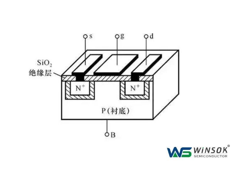
MOSFET internal structure
On a P-type silicon substrate with a low impurity concentration, two N+ regions with a high impurity concentration are made, and two electrodes are drawn out of metal aluminum to serve as the drain d and the source s respectively. Then the semiconductor surface is covered with an extremely thin silicon dioxide (SiO2) insulating layer, and an aluminum electrode is installed on the insulating layer between the drain and the source to serve as the gate g. An electrode B is also drawn out on the substrate, forming an N-channel enhancement-mode MOSFET. The same is true for the internal formation of P-channel enhancement-type MOSFETs.
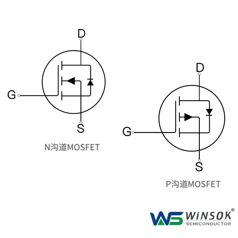
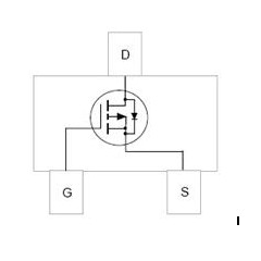
N-channel MOSFET and P-channel MOSFET circuit symbols
The picture above shows the circuit symbol of MOSFET. In the picture, D is the drain, S is the source, G is the gate, and the arrow in the middle represents the substrate. If the arrow points inward, it indicates an N-channel MOSFET, and if the arrow points outward, it indicates a P-channel MOSFET.
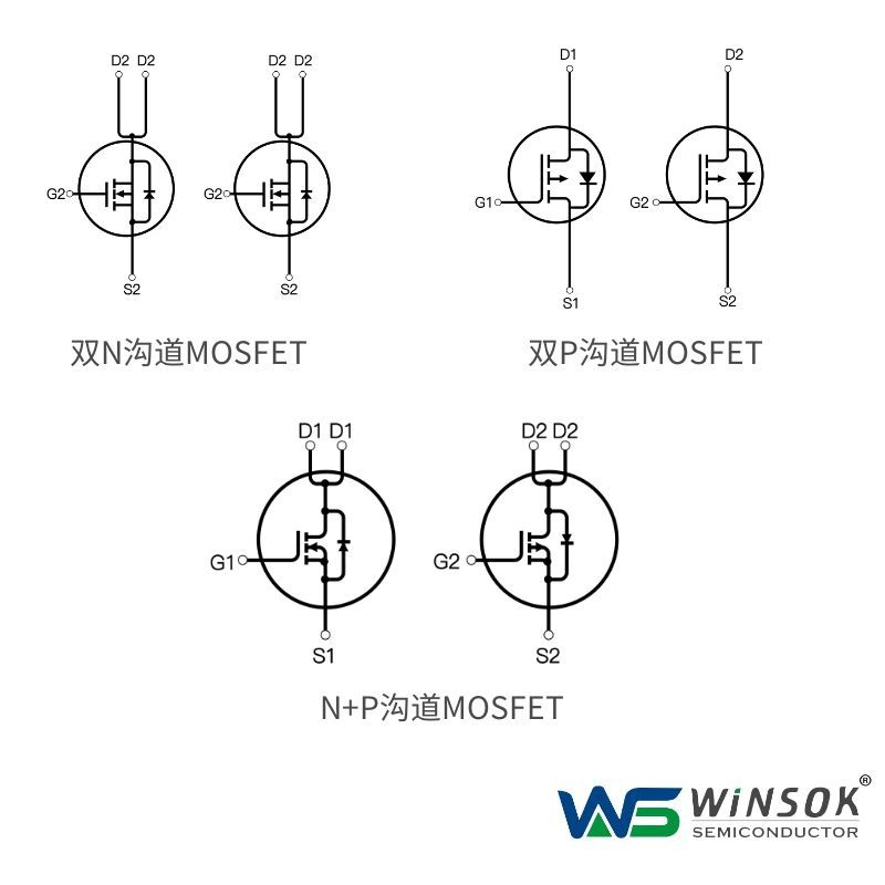
Dual N-channel MOSFET, dual P-channel MOSFET and N+P-channel MOSFET circuit symbols
In fact, during the MOSFET manufacturing process, the substrate is connected to the source before leaving the factory. Therefore, in the symbology rules, the arrow symbol representing the substrate must also be connected to the source to distinguish the drain and the source. The polarity of the voltage used by MOSFET is similar to our traditional transistor. The N-channel is similar to an NPN transistor. The drain D is connected to the positive electrode and the source S is connected to the negative electrode. When the gate G has a positive voltage, a conductive channel is formed and the N-channel MOSFET starts to work. Similarly, the P-channel is similar to a PNP transistor. The drain D is connected to the negative electrode, the source S is connected to the positive electrode, and when the gate G has a negative voltage, a conductive channel is formed and the P-channel MOSFET starts to work.
MOSFET switching loss principle
Whether it is NMOS or PMOS, there is a conduction internal resistance generated after it is turned on, so that the current will consume energy on this internal resistance. This part of the energy consumed is called conduction consumption. Selecting a MOSFET with a small conduction internal resistance will effectively reduce conduction consumption. The current internal resistance of low-power MOSFETs is generally around tens of milliohms, and there are also several milliohms.
When MOS is turned on and terminated, it must not be realized in an instant. The voltage on both sides of the MOS will have an effective decrease, and the current flowing through it will have an increase. During this period, the loss of the MOSFET is the product of the voltage and the current, which is the switching loss. Generally speaking, switching losses are much larger than conduction losses, and the faster the switching frequency, the greater the losses.
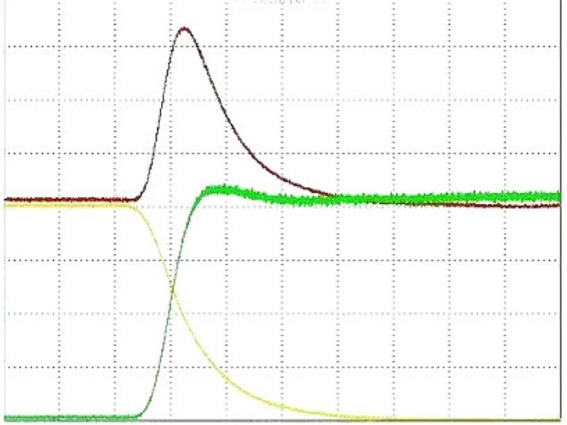
The product of voltage and current at the moment of conduction is very large, resulting in very large losses. Switching losses can be reduced in two ways. One is to reduce the switching time, which can effectively reduce the loss during each turn-on; the other is to reduce the switching frequency, which can reduce the number of switches per unit time.
The above is a detailed explanation of the working principle diagram of MOSFET and analysis of the internal structure of MOSFET. To learn more about MOSFET, welcome to consult OLUKEY to provide you with MOSFET technical support!


-
MOSFET Package Switching Tube Selection and Cir...
-

Analyzing Enhancement and Depletion MOSFETs
-

MOSFET Classification Characteristics
-

Important Steps on MOSFET Selection
-

Complete Guide to Optocoupler MOSFET Driver Cir...
-

MOSFET substitution principle and good and bad ...
-

Understanding MOSFET Overdrive Voltage: Compreh...
-

Using a MOSFET as a Switch: Complete Implementa...
-

TFET vs MOSFET: Understanding the Future of Tra...
-

Determining MOSFET Threshold Voltage: Expert Te...
-
Characteristics of MOSFETs and Precautions for Use
-

What Is Pinch-Off Voltage in MOSFETs? Key Conce...
-
How to choose the right package MOSFET?
-

Understanding Gate-to-Source Resistors in MOSFE...
-

MOSFET Selection | N-Channel MOSFET Constructio...
-

Common Gate MOSFET Amplifier: A Comprehensive A...


