


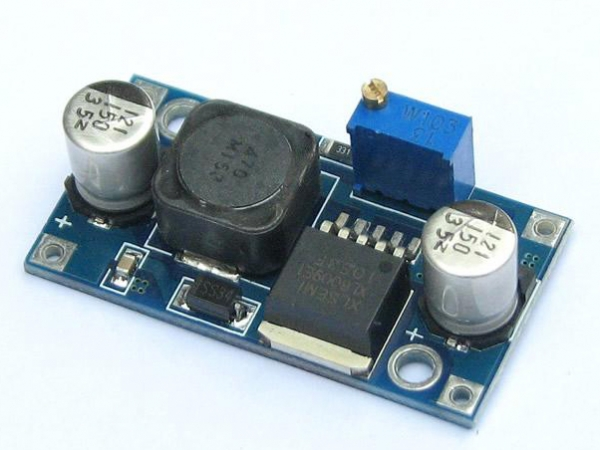
What is the role of MOSFETs?
MOSFETs play a role in regulating the voltage of the entire power supply system. Currently, there are not many MOSFETs used on the board, usually about 10. The main reason is that most of the MOSFETs are integrated into the IC chip. Since the main role of the MOSFET is to provide a stable voltage for the accessories, so it is generally used in the CPU, GPU and socket, etc. MOSFETs are generally above and below the form of a group of two appear on the board.
MOSFET Package
MOSFET chip in the production is completed, you need to add a shell to the MOSFET chip, that is, MOSFET package. MOSFET chip shell has a support, protection, cooling effect, but also for the chip to provide electrical connection and isolation, so that the MOSFET device and other components to form a complete circuit.
In accordance with the installation in the PCB way to distinguish, MOSFET package has two main categories: Through Hole and Surface Mount. inserted is the MOSFET pin through the PCB mounting holes welded on the PCB. Surface Mount is the MOSFET pin and heat sink flange welded to the PCB surface pads.
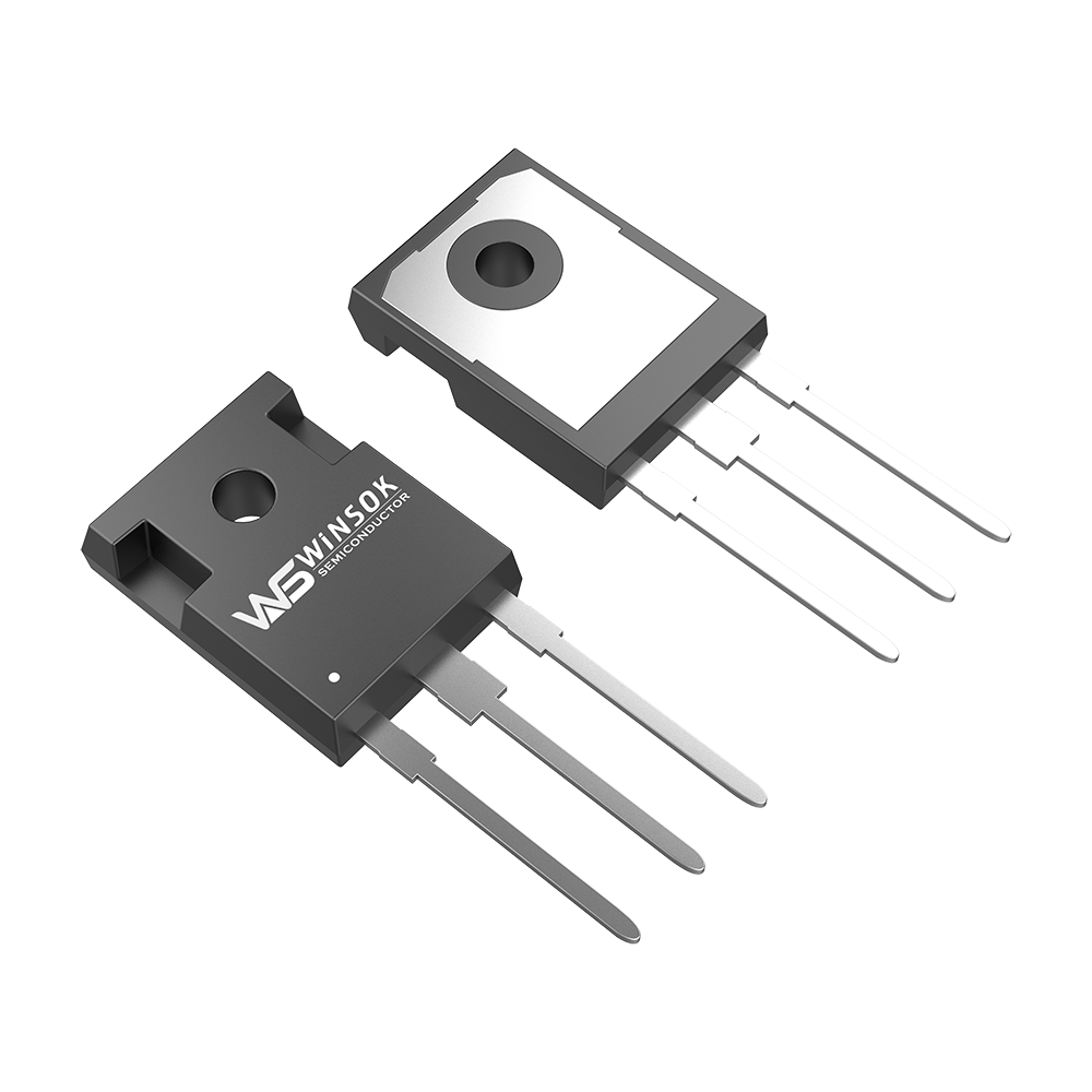
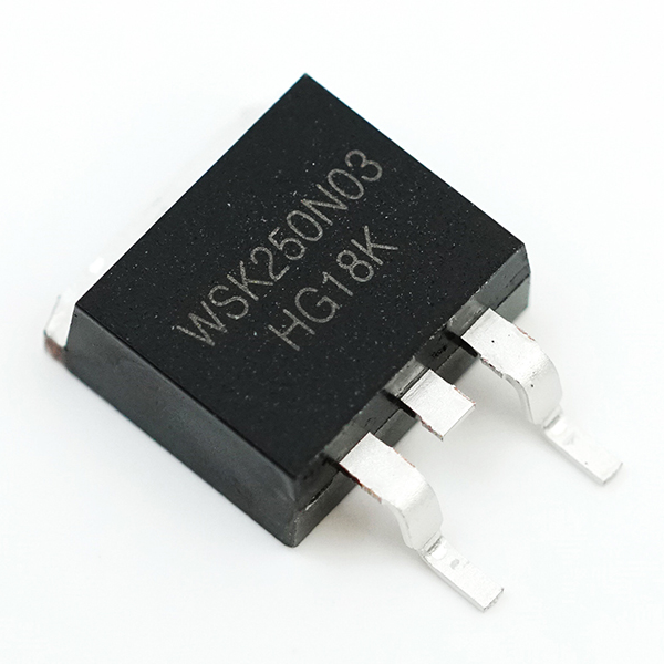
Standard Package Specifications TO Package
TO (Transistor Out-line) is the early package specification, such as TO-92, TO-92L, TO-220, TO-252, etc. are plug-in package design. In recent years, the surface mount market demand has increased, and TO packages have progressed to surface mount packages.
TO-252 and TO263 are surface mount packages. The TO-252 is also known as D-PAK and the TO-263 is also known as D2PAK.
D-PAK package MOSFET has three electrodes, gate (G), drain (D), source (S). One of the drain (D) pin is cut without using the back of the heat sink for the drain (D), directly welded to the PCB, on the one hand, for the output of high current, on the one hand, through the PCB heat dissipation. So there are three PCB D-PAK pads, the drain (D) pad is larger.
Package TO-252 pin diagram
Chip package popular or dual in-line package, referred to as DIP (Dual ln-line Package).DIP package at that time has a suitable PCB (printed circuit board) perforated installation, with easier than TO-type package PCB wiring and operation is more convenient and so on some of the characteristics of the structure of its package in the form of a number of forms, including multi-layer ceramic dual in-line DIP, single-layer Ceramic Dual In-Line
DIP, lead frame DIP and so on. Commonly used in power transistors, voltage regulator chip package.
Chip MOSFET Package
SOT Package
SOT (Small Out-Line Transistor) is a small outline transistor package. This package is a SMD small power transistor package, smaller than the TO package, generally used for small power MOSFET.
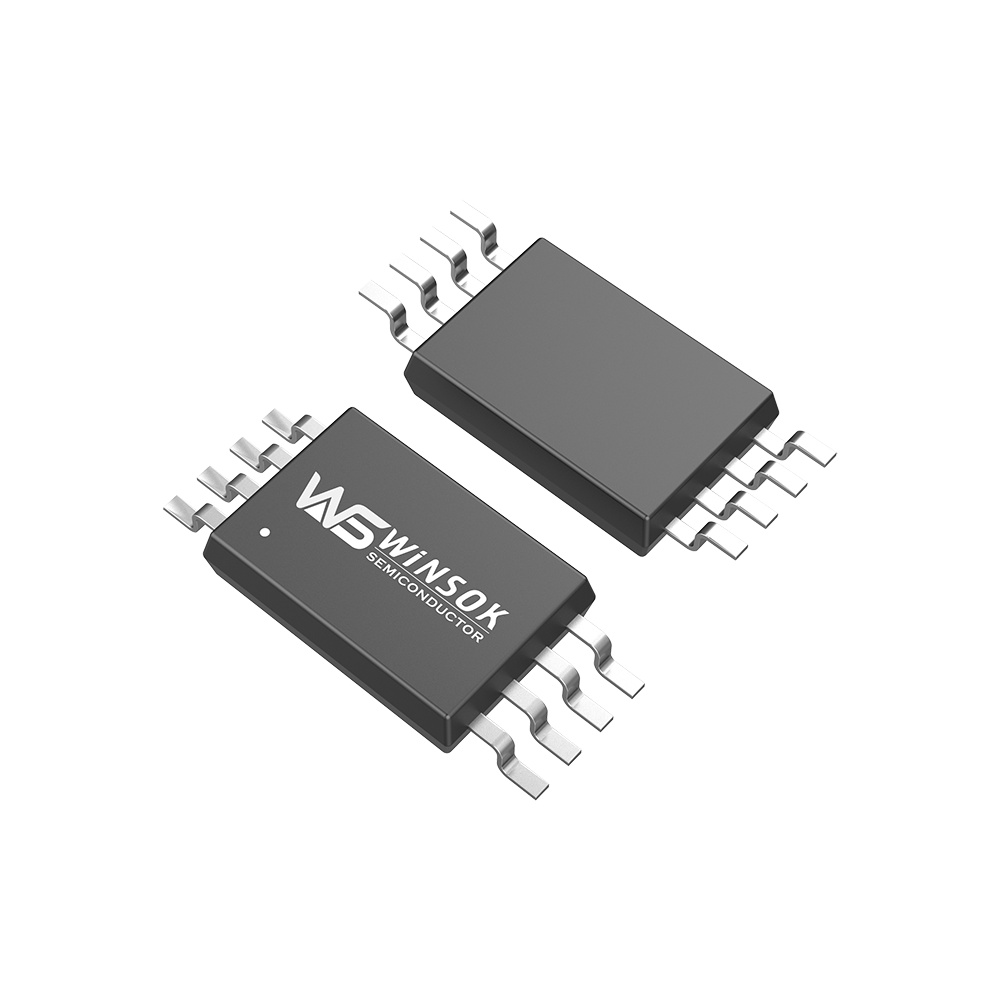
SOP Package
SOP (Small Out-Line Package) means "Small Outline Package" in Chinese, SOP is one of the surface mount packages, the pins from the two sides of the package in the shape of a gull's wing (L-shaped), the material is plastic and ceramic. SOP is also called SOL and DFP. SOP package standards include SOP-8, SOP-16, SOP-20, SOP-28, etc. The number after SOP indicates the number of pins.
The SOP package of MOSFET mostly adopts SOP-8 specification, the industry tends to omit the "P", called SO (Small Out-Line).
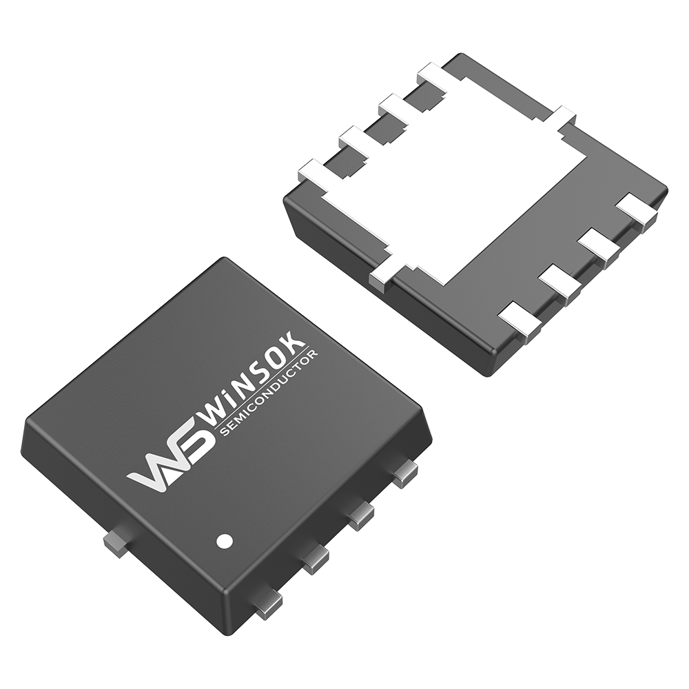
SMD MOSFET Package
SO-8 plastic package, there is no thermal base plate, poor heat dissipation, generally used for low-power MOSFET.
SO-8 was first developed by PHILIP, and then gradually derived from TSOP (thin small outline package), VSOP (very small outline package), SSOP (reduced SOP), TSSOP (thin reduced SOP) and other standard specifications.
Among these derived package specifications, TSOP and TSSOP are commonly used for MOSFET packages.
Chip MOSFET Packages
QFN (Quad Flat Non-leaded package) is one of the surface mount packages, the Chinese called the four-side non-leaded flat package, is a pad size is small, small, plastic as the sealing material of the emerging surface mount chip packaging technology, now more commonly known as LCC. It is now called LCC, and QFN is the name stipulated by the Japan Electrical and Mechanical Industries Association. The package is configured with electrode contacts on all sides.
The package is configured with electrode contacts on all four sides, and since there are no leads, the mounting area is smaller than QFP and the height is lower than that of QFP. This package is also known as LCC, PCLC, P-LCC, etc.
-

Analysis of the reasons for the ineffectiveness...
-
What is the principle of operation of MOSFET?
-

Briefly talk about the production method of a h...
-
MOSFETs in Electric Vehicle Controllers
-

Recognition of Insulated Layer Gate MOSFETs
-

What are the main features of MOSFETs?
-
MOSFET small current heating causes and measures
-

2N2222 Transistor: The Versatile Workhorse of E...
-
Introduction to the working principle of common...
-

The importance of power MOSFET in motherboard d...
-

The difference between N-channel MOSFET and P-c...
-

Did you know about the evolution of MOSFET?
-

CMS32L051SS24 MCU Cmsemicon® Package SSOP24 Bat...
-

MOSFET conduction characteristics
-

Detailed explanation of the working principle d...
-

How much do you know about MOSFET parameters? O...


