


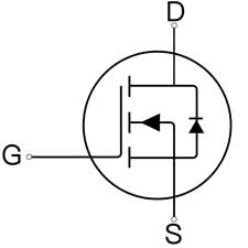
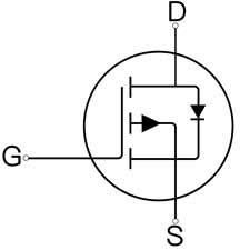
There are many variations of circuit symbols commonly used for MOSFETs. The most common design is a straight line representing the channel, two lines perpendicular to the channel representing the source and drain, and a shorter line parallel to the channel on the left representing the gate. Sometimes the straight line representing the channel is also replaced by a broken line to distinguish between enhancement mode mosfet or depletion mode mosfet, which is also divided into N-channel MOSFET and P-channel MOSFET two types of circuit symbols as shown in the figure (the direction of the arrow is different).
Power MOSFETs work in two main ways:
(1) When a positive voltage is added to D and S (drain positive, source negative) and UGS=0, the PN junction in the P body region and the N drain region is reverse biased, and there is no current passing between D and S. If a positive voltage UGS is added between G and S, no gate current will flow because the gate is insulated, but a positive voltage at the gate will push the holes away from the P region underneath, and the minority carrier electrons will be attracted to the P region surface When the UGS is greater than a certain voltage UT, the electron concentration on the surface of the P region under the gate will exceed the hole concentration, thus making the P-type semiconductor antipattern layer N-type semiconductor; this antipattern layer forms an N-type channel between the source and drain, so that the PN junction disappears, the source and drain conductive, and a drain current ID flows through the drain. UT is called the turn-on voltage or the threshold voltage, and the more UGS exceeds UT, the more conductive the conductive capability is, and the larger the ID is. The greater the UGS exceeds UT, the stronger the conductivity, the greater the ID.
(2) When D, S plus negative voltage (source positive, drain negative), the PN junction is forward biased, equivalent to an internal reverse diode (does not have a fast response characteristics), that is, the MOSFET does not have reverse blocking capability, can be regarded as an inverse conduction components.
By the MOSFET principle of operation can be seen, its conduction only one polarity carriers involved in the conductive, so also known as unipolar transistor.MOSFET drive is often based on the power supply IC and MOSFET parameters to select the appropriate circuit, MOSFET is generally used for switching power supply drive circuit. When designing a switching power supply using a MOSFET, most people consider the on-resistance, maximum voltage, and maximum current of the MOSFET. However, people very often only consider these factors, so that the circuit can work properly, but it is not a good design solution. For a more detailed design, the MOSFET should also consider its own parameter information. For a definite MOSFET, its driving circuit, the peak current of the drive output, etc., will affect the switching performance of the MOSFET.
Post time: May-17-2024


