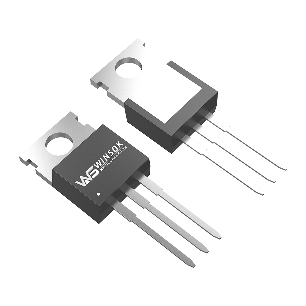
Explore the unique characteristics and applications of N-Channel depletion mode MOSFETs with Olukey, your authorized distributor of Winsok’s advanced semiconductor solutions. Understand how these specialized components can enhance your circuit designs with their normally-on characteristics and distinctive operational features.
Understanding Depletion Mode MOSFET Fundamentals
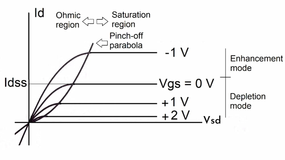
Unlike enhancement mode MOSFETs, depletion mode devices are normally-on at zero gate-source voltage, offering unique advantages in specific circuit applications. This fundamental characteristic stems from their physical structure and fabrication process.
Key Characteristics
- Normally-on operation (conducts at VGS = 0V)
- Requires negative gate voltage for turn-off
- Built-in channel during fabrication
- Higher current handling capability at zero gate bias
- Unique transfer characteristics curve
Operating Regions and Characteristics
Cut-off Region
VGS < VP (Pinch-off voltage)
- Channel fully depleted
- No current flow
- Device acts as open circuit
Linear Region
VGS > VP and VDS < VGS – VP
- Channel partially depleted
- Device acts as voltage-controlled resistor
- Linear I-V characteristics
Saturation Region
VGS > VP and VDS > VGS – VP
- Channel pinched off at drain end
- Current remains constant
- Ideal for amplification
Mathematical Model and Equations
Linear Region Current Equation:
ID = IDSS(1 – VGS/VP)²[2(VDS/VP) - (VDS/VP)²]
Saturation Region Current Equation:
ID = IDSS(1 – VGS/VP)²
Where:
- IDSS = Saturated drain current at VGS = 0V
- VP = Pinch-off voltage (negative for n-channel)
- VGS = Gate-to-source voltage
- VDS = Drain-to-source voltage
Winsok’s N-Channel Depletion MOSFET Portfolio
| Model | IDSS (mA) | VP (V) | RDS(on) (Ω) | Applications |
|---|---|---|---|---|
| WS-DN100 | 10-15 | -2.5 | 50 | Low-power amplifiers |
| WS-DN200 | 20-30 | -3.0 | 35 | Current sources |
| WS-DN300 | 50-75 | -4.0 | 20 | Power supplies |
| WS-DN400 | 100-150 | -5.0 | 10 | High-power applications |
Selecting the Right Depletion Mode MOSFET
Choosing the appropriate depletion mode MOSFET requires careful consideration of multiple parameters and application requirements. Here’s a comprehensive selection guide to help you make informed decisions.
Primary Selection Parameters
| Parameter | Description | Selection Considerations |
|---|---|---|
| IDSS | Zero-gate drain current |
|
| VP (Pinch-off Voltage) | Gate voltage required to turn off the device |
|
| RDS(on) | On-state resistance |
|
| Ciss, Coss, Crss | Input, output, and reverse transfer capacitances |
|
Application-Specific Selection Guide
Constant Current Source Applications
- Key Parameters:
- IDSS tolerance
- Temperature coefficient
- Output impedance
- Recommended Model: WS-DN200 Series
- ±5% IDSS tolerance
- Optimized temperature characteristics
High-Frequency Applications
- Key Parameters:
- Input/output capacitances
- Switching characteristics
- Gate charge
- Recommended Model: WS-DN300 Series
- Low gate charge
- Optimized for RF applications
Power Applications
- Key Parameters:
- Power dissipation
- Safe operating area
- Thermal resistance
- Recommended Model: WS-DN400 Series
- Enhanced thermal performance
- Robust SOA characteristics
Selection Process Workflow
- Define Application Requirements
- Operating current range
- Voltage requirements
- Frequency of operation
- Temperature range
- Calculate Safety Margins
- Current derating (30% recommended)
- Voltage derating (50% recommended)
- Temperature derating
- Consider Secondary Parameters
- Package requirements
- Thermal considerations
- Cost constraints
- Verify Device Availability
- Production status
- Lead time
- Alternative sources
Key Selection Calculations
Maximum Operating Current: Iop_max = IDSS × 0.7
Power Dissipation: PD = ID² × RDS(on) + VGS × IG
Temperature Rise: ΔT = PD × RθJA
Need Help Selecting the Right Depletion Mode MOSFET?
Our technical team at Olukey can assist you in choosing the optimal Winsok depletion mode MOSFET for your specific application. We provide:
- Detailed technical consultation
- Sample evaluation support
- Application-specific recommendations
- Performance optimization guidance
Common Selection Pitfalls to Avoid
- Overlooking temperature effects on IDSS
- Insufficient voltage margins for VGS
- Inadequate consideration of switching requirements
- Neglecting package thermal limitations
- Ignoring long-term reliability factors
Application Circuits and Design Considerations
Constant Current Source
One of the most common applications of depletion-mode MOSFETs is as a constant current source:
- Self-biasing capability
- High output impedance
- Temperature stability considerations
- Circuit stabilization techniques
Cascode Amplifiers
Advantages in cascode configurations:
- Improved frequency response
- Reduced Miller effect
- Higher output impedance
- Better isolation
Level Shifters
Benefits in level shifting applications:
- Wide voltage range handling
- Low power consumption
- High-speed operation
- Simple implementation
Protection Circuits
Usage in protection schemes:
- Overcurrent protection
- Voltage clamping
- Fail-safe operation
- Quick response time
Practical Design Considerations
Temperature Effects
Critical parameters affected by temperature:
- Threshold voltage drift
- Channel mobility variations
- Leakage current changes
- Performance degradation considerations
| Parameter | Temperature Coefficient | Compensation Method |
|---|---|---|
| Threshold Voltage | -2mV/°C | Temperature sensing feedback |
| Mobility | -0.7%/°C | Current mirror compensation |
| On-Resistance | 0.7%/°C | Active biasing network |
Advanced Applications
RF Circuit Applications
- Mixer circuits
- RF amplifiers
- Impedance matching networks
- Frequency multipliers
Analog Signal Processing
- Variable gain amplifiers
- Active filters
- Sample and hold circuits
- Analog multiplexers
Power Management
- DC-DC converters
- Linear regulators
- Battery charging circuits
- Power distribution
Reliability and Lifetime Considerations
Critical Reliability Factors
- Gate oxide integrity
- Hot carrier effects
- Thermal cycling endurance
- ESD protection requirements
- Operating environment considerations
Expert Support for Your Depletion Mode MOSFET Applications
Partner with Olukey for access to Winsok’s premium N-channel depletion mode MOSFETs and comprehensive technical support. Our engineering team is ready to assist with your specific application requirements.
Quality Assurance and Testing
Winsok Testing Standards
- 100% production testing
- Statistical process control
- Environmental stress screening
- Reliability qualification
- Failure analysis capabilities
Ready to optimize your circuit design with depletion mode MOSFETs?


