Understanding MOSFET Overdrive Voltage: Fundamental Concepts
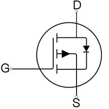
MOSFET overdrive voltage (VOV), defined as the difference between the gate-to-source voltage (VGS) and the threshold voltage (VTH), plays a crucial role in determining MOSFET operation and performance characteristics. This comprehensive analysis explores the theoretical foundations, practical implications, and optimization strategies for MOSFET overdrive voltage.
Basic Overdrive Voltage Formula and Relationships
Key Formulas:
VOV = VGS – VTH
ID = K × (VOV)² × (1 + λVDS) [in saturation region]
ID = K × [2(VOV)VDS - VDS²] [in linear region]
Where:
- VOV = Overdrive voltage
- VGS = Gate-to-source voltage
- VTH = Threshold voltage
- ID = Drain current
- K = Transconductance parameter
- λ = Channel-length modulation parameter
- VDS = Drain-to-source voltage
Impact of Overdrive Voltage on MOSFET Parameters
| Parameter | Low Overdrive Voltage | High Overdrive Voltage | Optimal Range (Winsok MOSFETs) |
|---|---|---|---|
| On-Resistance (RDS(on)) | Higher | Lower | 2-5mΩ @ VOV = 4V |
| Switching Speed | Slower | Faster | 10-30ns @ VOV = 5V |
| Power Dissipation | Higher in linear region | Lower in linear region | Optimized @ VOV = 3-6V |
| Transconductance (gm) | Lower | Higher | 20-40 S @ VOV = 5V |
Operating Regions and Overdrive Voltage
Cut-off Region
VGS < VTH
No channel formation
Minimal leakage current
Linear Region
VGS > VTH
VDS < VOV
Channel acts as resistor
Saturation Region
VGS > VTH
VDS ≥ VOV
Current nearly independent of VDS
Advanced Analysis of Overdrive Voltage Effects
Temperature Dependencies
The relationship between overdrive voltage and temperature is critical for reliable MOSFET operation:
| Temperature Effect | Impact on Parameters | Compensation Strategy |
|---|---|---|
| VTH Reduction | -2mV/°C to -4mV/°C | Temperature-compensated biasing |
| Mobility Degradation | Reduced current capability | Increased VOV at higher temperatures |
| RDS(on) Variation | Positive temperature coefficient | Design margin in VOV selection |
Frequency Response and Switching Behavior
Dynamic Parameters vs. Overdrive Voltage
Winsok’s advanced MOSFET technology optimizes these crucial switching parameters:
- Turn-on delay time (td(on)) ∝ 1/VOV
- Rise time (tr) ∝ 1/VOV
- Turn-off delay time (td(off)) ∝ VOV
- Fall time (tf) ∝ 1/VOV
Design Considerations for Optimal Overdrive Voltage
Circuit Design Parameters
Power Efficiency
Higher overdrive voltage reduces conduction losses but increases switching losses. Optimal VOV depends on operating frequency and load conditions.
Reliability Margins
Consider temperature effects, component tolerances, and aging factors when selecting overdrive voltage.
EMI Considerations
Balance switching speed with EMI requirements through proper overdrive voltage selection.
Application-Specific Optimization
| Application | Typical VOV Range | Key Considerations | Recommended Winsok Series |
|---|---|---|---|
| Switch-Mode Power Supplies | 4-6V | Efficiency vs. switching losses | WS-PowerSwitch™ Series |
| Motor Drivers | 5-8V | Low RDS(on), thermal management | WS-DriveForce™ Series |
| Battery Management | 3-5V | Power consumption, protection | WS-BatGuard™ Series |
| RF Applications | 2-4V | Linearity, bandwidth | WS-RFMaster™ Series |
Advanced Design Techniques and Considerations
Gate Drive Circuit Optimization
- Implementation of adaptive gate drive voltage control
- Temperature-compensated gate drive circuits
- Active Miller clamp techniques
- Resonant gate drive solutions
Winsok’s Advanced MOSFET Solutions
Our latest generation MOSFETs feature:
- Advanced trench gate technology for optimized overdrive characteristics
- Integrated temperature sensing and protection
- Enhanced short-circuit capability
- Superior dv/dt immunity
Mathematical Analysis and Performance Optimization
Key Performance Equations
Advanced Formulas for Circuit Analysis:
Power Dissipation: PD = ID² × RDS(on) + (QG × VGS × f)
Transconductance: gm = (2 × ID × K)^0.5
Switching Energy: ESW = 0.5 × VDS × ID × (tr + tf)
Gate Charge Relationship: QG = CGS × VGS + CGD × (VGS + VDS)
Practical Implementation Guidelines
Design Verification
Comprehensive testing procedures including temperature cycling, load variation, and EMI compliance.
Thermal Management
Advanced cooling solutions and thermal design considerations for optimal performance.
Protection Schemes
Implementation of overcurrent, overvoltage, and thermal protection mechanisms.
Expert Support and Solutions
Olukey provides comprehensive support for implementing Winsok’s MOSFET solutions in your applications:
- Detailed application notes and design guidelines
- SPICE models for circuit simulation
- Technical consultation and design review services
- Prototype development support
Ready to Optimize Your MOSFET Applications?
Let Olukey’s expert team help you select the perfect Winsok MOSFET solution for your specific requirements. Our comprehensive support ensures optimal overdrive voltage implementation for maximum performance and reliability.
For detailed specifications, application support, or to discuss your specific requirements, please contact our technical sales team. Our engineering experts are ready to assist you in optimizing your MOSFET-based designs.


