
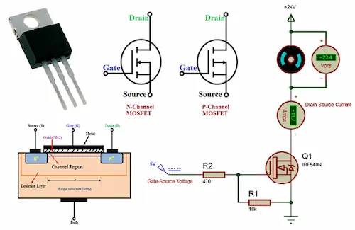
Terminal Configuration Fundamentals
Gate Terminal
Controls the formation of the conduction channel through electric field effect. The gate voltage determines the MOSFET’s switching state and conductivity.
Drain Terminal
Primary current input terminal in N-channel MOSFETs. The drain typically connects to the higher potential in the circuit.
Source Terminal
Reference terminal for gate voltage and current output path. Usually connected to circuit ground in N-channel configurations.
Critical Operating Parameters
| Parameter | Symbol | Description | Typical Range |
|---|---|---|---|
| Gate Threshold Voltage | VGS(th) | Minimum gate voltage needed to create a conducting channel | 2-4V |
| Drain-Source Voltage | VDS | Maximum voltage between drain and source | 30-800V |
| Gate-Source Voltage | VGS | Operating voltage applied to gate relative to source | ±10-20V |
Operating Regions and Characteristics
Cut-off Region
VGS < VGS(th)
MOSFET is OFF, minimal drain current flows
Linear Region
VGS > VGS(th) and VDS < VGS – VGS(th)
MOSFET acts as a voltage-controlled resistor
Saturation Region
VGS > VGS(th) and VDS > VGS – VGS(th)
MOSFET operates as a constant current source
Practical Application Considerations
 As an authorized MOSFET distributor, we’ve observed that successful implementation requires careful attention to terminal characteristics and protection mechanisms.
Gate Protection
- Use gate resistors (typical values: 10Ω – 100Ω)
- Include TVS diodes for voltage spikes
- Consider Zener clamps for voltage limitation
Source Considerations
- Implement Kelvin source connection
- Minimize source inductance
- Consider thermal management requirements
Drain Circuit Design
- Use snubber networks for voltage spikes
- Consider parasitic capacitances
- Implement proper thermal paths
Terminal Layout Best Practices
PCB Layout Guidelines
- Minimize gate loop area to reduce inductance
- Separate power and signal grounds
- Use wide traces for drain current path
- Place gate driver components close to MOSFET
Common Configuration Scenarios
| Configuration | Application | Key Considerations |
|---|---|---|
| Low-Side Switch | Ground-referenced loads | Simple gate drive, direct source grounding |
| High-Side Switch | Bridge circuits, motor drives | Floating gate drive required, bootstrap considerations |
| Synchronous Buck | DC-DC conversion | Dead-time management, body diode conduction |
Temperature Effects on Terminal Behavior
- Gate threshold voltage decreases with temperature
- On-resistance increases with temperature
- Switching speeds affected by temperature changes
- Leakage currents increase at higher temperatures
Troubleshooting Common Issues
Gate Issues
Symptoms: Slow switching, oscillations, damage
Solutions: Check gate resistance, drive voltage, layout
Drain-Source Problems
Symptoms: Excessive heating, voltage spikes
Solutions: Verify snubber design, thermal management
Source Connection Issues
Symptoms: False triggering, noise sensitivity
Solutions: Improve grounding, check Kelvin connection
Advanced Design Optimization
 Modern MOSFET designs require careful balance of:
- Switching speed vs. EMI generation
- Conduction losses vs. die size
- Gate charge vs. switching losses
- Thermal management vs. power density
Why Choose Olukey for Your MOSFET Needs?
- Authorized distributor of premium Winsok MOSFETs
- Comprehensive technical support and design consultation
- Extensive inventory for immediate availability
- Competitive pricing and flexible order quantities
- Quality assurance and reliability testing


-

Detailed explanation of the working principle d...
-

Stacking MOSFETs for Enhanced Gain: Advanced De...
-

Power MOSFET Avalanche Guidelines: Ensuring Rel...
-

Ideas to solve the serious heat generation of M...
-

MOSFET Solid State Relays: Revolutionizing Mode...
-
MOSFET small current heating causes and measures
-

Analyzing Enhancement and Depletion MOSFETs
-
What is the principle of operation of MOSFET?
-
Why is it always difficult to test high power M...
-

How Long Do MOSFETs Last? A Comprehensive Guide...
-

MOSFET Voltage-Controlled Resistor: Advanced Ap...
-

CMS8H1213 MCU Cmsemicon® Package SSOP24 Batch 24+
-

How much do you know about the MOSFET model cro...
-

Understanding CMOS Switch Technology: From Basi...
-
Understand the working principle of MOSFET and ...
-

Do You Know About MOSFET Circuits?


