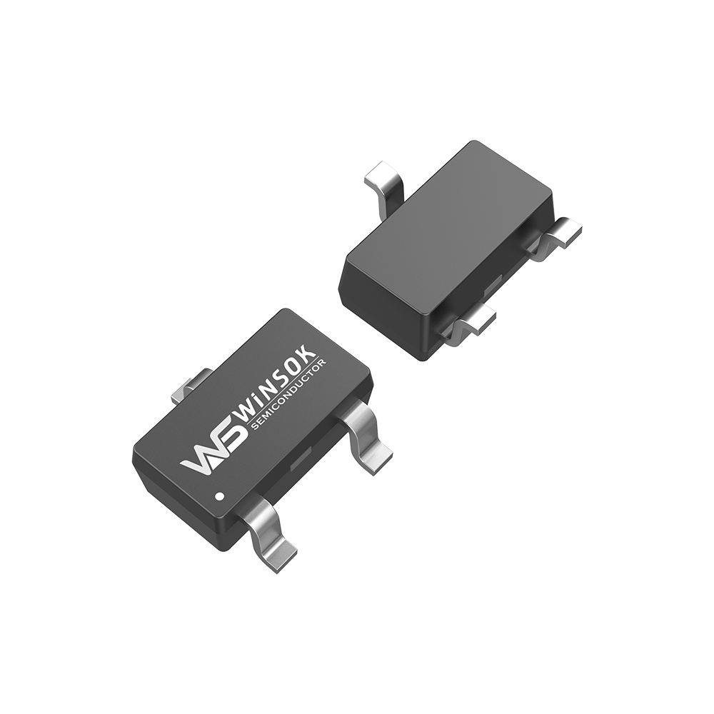
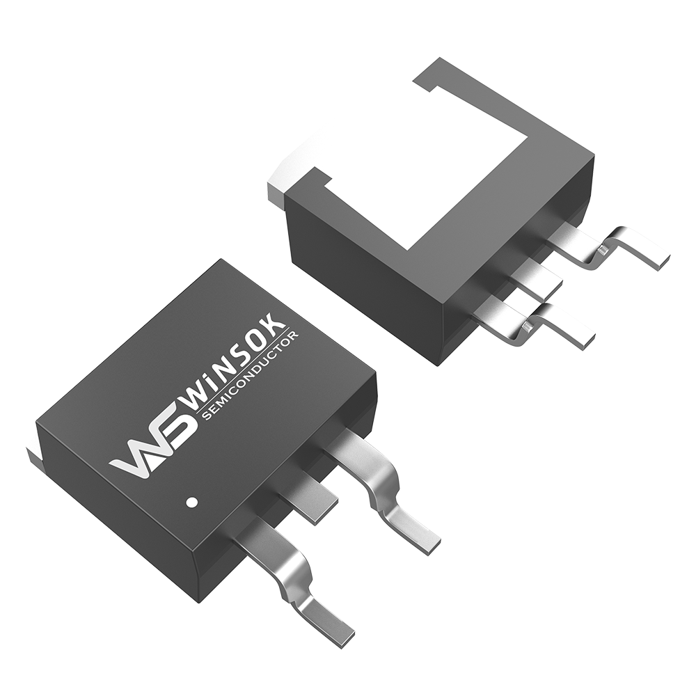
The MOSFET anti-reverse circuit is a protection measure used to prevent the load circuit from being damaged by reverse power polarity. When the power supply polarity is correct, the circuit works normally; when the power supply polarity is reversed, the circuit is automatically disconnected, thus protecting the load from damage. The following is a detailed analysis of the MOSFET anti-reverse circuit:

First, the basic principle of the MOSFET anti-reverse circuit
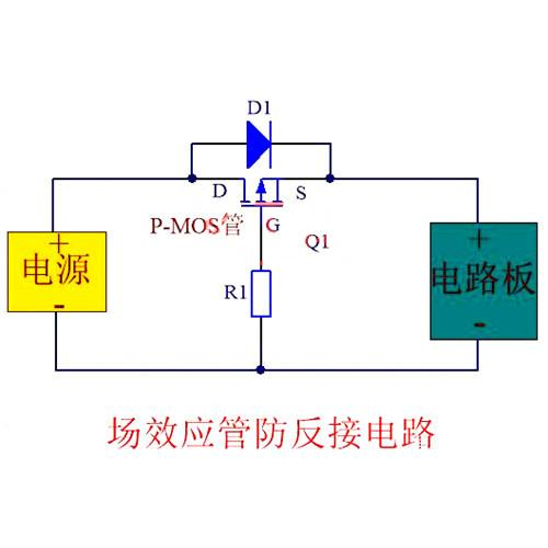
MOSFET anti-reverse circuit using the switching characteristics of the MOSFET, by controlling the gate (G) voltage to realize the circuit on and off. When the power supply polarity is correct, the gate voltage makes the MOSFET in the conduction state, the current can flow normally; when the power supply polarity is reversed, the gate voltage can not make the MOSFET conduction, thus cutting off the circuit.
Second, the specific realization of the MOSFET anti-reverse circuit
1. N-channel MOSFET anti-reverse circuit
N-channel MOSFETs are usually used to realize anti-reverse circuits. In the circuit, the source (S) of the N-channel MOSFET is connected to the negative terminal of the load, the drain (D) is connected to the positive terminal of the power supply, and the gate (G) is connected to the negative terminal of the power supply through a resistor or controlled by a control circuit.
Forward connection: the positive terminal of the power supply is connected to D, and the negative terminal is connected to S. At this time, the resistor provides the gate source voltage (VGS) for the MOSFET, and when VGS is greater than the threshold voltage (Vth) of the MOSFET, the MOSFET conducts, and the current flows from the positive terminal of the power supply to the load through the MOSFET.
When reversed: the positive terminal of the power supply is connected to S, and the negative terminal is connected to D. At this time, the MOSFET is in a cutoff state and the circuit is disconnected to protect the load from damage because the gate voltage is not able to form a sufficient VGS to make the MOSFET conduct (VGS may be less than 0 or much less than Vth).
2. Role of Auxiliary Components
Resistor: Used to provide gate source voltage for MOSFET and limit gate current to prevent gate overcurrent damage.
Voltage regulator: an optional component used to prevent the gate source voltage from being too high and breaking down the MOSFET.
Parasitic Diode: A parasitic diode (body diode) exists inside the MOSFET, but its effect is usually ignored or avoided by circuit design to avoid its detrimental effect in anti-reverse circuits.
Third, the advantages of the MOSFET anti-reverse circuit
Low loss: MOSFET on-resistance is small, the on-resistance voltage is reduced, so the circuit loss is small.
High reliability: anti-reverse function can be realized through a simple circuit design, and the MOSFET itself has a high degree of reliability.
Flexibility: different MOSFET models and circuit designs can be selected to meet different application requirements.
Precautions
In the design of MOSFET anti-reverse circuit, you need to ensure that the selection of MOSFETs to meet the application requirements, including voltage, current, switching speed and other parameters.
It is necessary to consider the influence of other components in the circuit, such as parasitic capacitance, parasitic inductance, etc., in order to avoid adverse effects on the circuit performance.
In practical applications, adequate testing and verification are also required to ensure the stability and reliability of the circuit.
In summary, the MOSFET anti-reverse circuit is a simple, reliable and low-loss power supply protection scheme that is widely used in a variety of applications that require the prevention of reverse power polarity.


