Parameters such as gate capacitance and on-resistance of a MOSFET (Metal-Oxide-Semiconductor Field-Effect Transistor) are important indicators for evaluating its performance. The following is a detailed explanation of these parameters:

I. Gate capacitance
Gate capacitance mainly includes input capacitance (Ciss), output capacitance (Coss) and reverse transfer capacitance (Crss, also known as Miller capacitance).
Input Capacitance (Ciss):
DEFINITION: The input capacitance is the total capacitance between the gate and the source and drain, and consists of the gate source capacitance (Cgs) and the gate drain capacitance (Cgd) connected in parallel, i.e. Ciss = Cgs + Cgd.
Function: The input capacitance affects the switching speed of the MOSFET. When the input capacitance is charged to a threshold voltage, the device can be turned on; discharged to a certain value, the device can be turned off. Therefore, the driving circuit and Ciss have a direct impact on the device's turn-on and turn-off delay.
Output capacitance (Coss):
Definition: The output capacitance is the total capacitance between the drain and the source, and consists of the drain-source capacitance (Cds) and the gate-drain capacitance (Cgd) in parallel, i.e. Coss = Cds + Cgd.
Role: In soft-switching applications, Coss is very important because it may cause resonance in the circuit.
Reverse Transmission Capacitance (Crss):
Definition: The reverse transfer capacitance is equivalent to the gate drain capacitance (Cgd) and is often referred to as the Miller capacitance.
Role: The reverse transfer capacitance is an important parameter for the rise and fall times of the switch, and it also affects the turn-off delay time. The capacitance value decreases as the drain-source voltage increases.
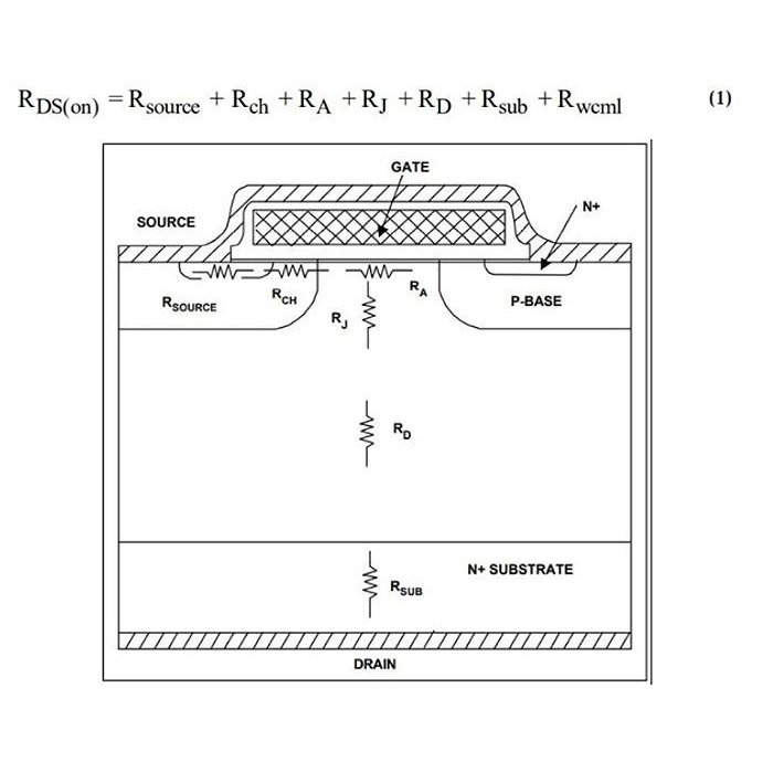
II. On-resistance (Rds(on))
Definition: On-resistance is the resistance between the source and drain of a MOSFET in the on-state under specific conditions (e.g., specific leakage current, gate voltage, and temperature).
Influencing factors: On-resistance is not a fixed value, it is affected by temperature, the higher the temperature, the greater the Rds(on). In addition, the higher the withstand voltage, the thicker the internal structure of the MOSFET, the higher the corresponding on-resistance.
Importance: When designing a switching power supply or driver circuit, it is necessary to consider the on-resistance of the MOSFET, because the current flowing through the MOSFET will consume energy on this resistance, and this part of the consumed energy is called on-resistance loss. Selecting a MOSFET with low on-resistance can reduce the on-resistance loss.
Third, other important parameters
In addition to the gate capacitance and on-resistance, the MOSFET has some other important parameters such as:
V(BR)DSS (Drain Source Breakdown Voltage): The drain source voltage at which the current flowing through the drain reaches a specific value at a specific temperature and with the gate source shorted. Above this value, the tube may be damaged.
VGS(th) (Threshold Voltage): The gate voltage required to cause a conducting channel to begin to form between the source and drain. For standard N-channel MOSFETs, VT is about 3 to 6V.
ID (Maximum Continuous Drain Current): The maximum continuous DC current that can be allowed by the chip at the maximum rated junction temperature.
IDM (Maximum Pulsed Drain Current): Reflects the level of pulsed current that the device can handle, with pulsed current being much higher than continuous DC current.
PD (maximum power dissipation): the device can dissipate the maximum power consumption.
In summary, the gate capacitance, on-resistance and other parameters of a MOSFET are critical to its performance and application, and need to be selected and designed according to specific application scenarios and requirements.


