
As a leading MOSFET supplier, we often receive inquiries about implementing logic gates using MOSFETs. This guide demonstrates how to construct a reliable OR gate using MOSFETs, with practical considerations for real-world applications.
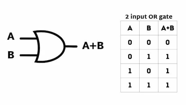
Understanding OR Gate Logic
| Input A | Input B | Output |
|---|---|---|
| 0 | 0 | 0 |
| 0 | 1 | 1 |
| 1 | 0 | 1 |
| 1 | 1 | 1 |
Required Components
Core Components
- 2x N-channel MOSFETs
- 1x Pull-down resistor (10kΩ)
- 2x Input protection resistors (1kΩ)
Power Supply
- VDD: 5V DC supply
- Ground connection
- Bypass capacitor (0.1µF)
Optional Components
- Input protection diodes
- Output buffer
- LED indicator
Implementation Steps
Circuit Layout Preparation
Start with a clean breadboard or PCB area. Establish separate power and ground rails. Place bypass capacitors near the power supply connection points.
MOSFET Placement
Position the two N-channel MOSFETs parallel to each other. Connect their drain terminals together – this will be your output node.
Source Connections
Connect both MOSFET source terminals to ground. Ensure low-impedance paths to minimize source degeneration effects.
Gate Circuit Implementation
Add 1kΩ gate resistors to each MOSFET gate. These serve as input protection and help prevent oscillations.
Pull-down Configuration
Install the 10kΩ pull-down resistor between the common drain connection and ground.
Circuit Configuration Details
- Power supply (VDD): Connect to drain through pull-up resistor
- Inputs A & B: Connect to respective gate resistors
- Output: Taken from common drain connection
- Ground: Common reference for all components
Important Considerations:
- Use MOSFETs with similar threshold voltages
- Keep gate connections short to minimize inductance
- Consider adding input protection diodes for sensitive applications
- Monitor heat dissipation during continuous operation
Performance Optimization
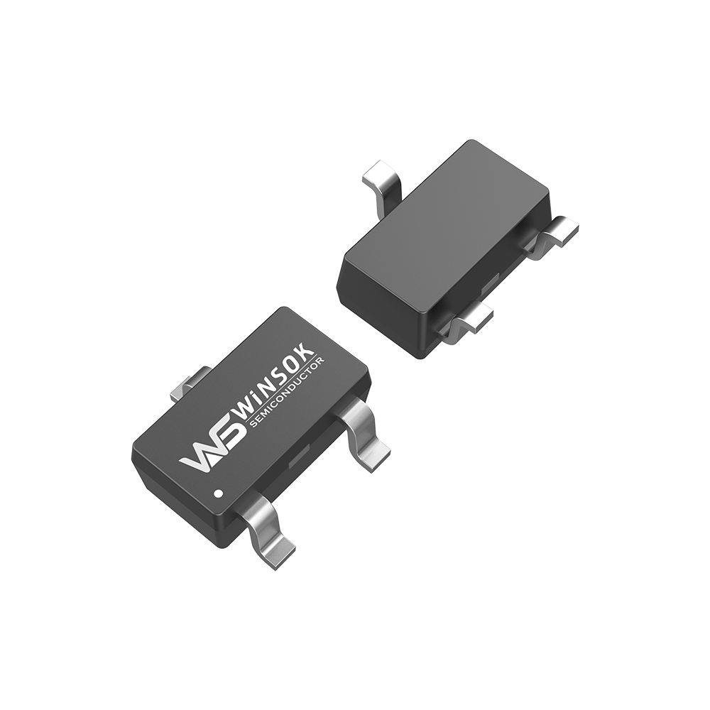
 Pro Tip: For optimal switching performance, we recommend using Winsok’s WSF series MOSFETs, available through Olukey, which offer:
- Low RDS(on) for minimal conduction losses
- Fast switching speeds
- Excellent thermal characteristics
- Built-in ESD protection
Troubleshooting Guide
Common Issues and Solutions:
| Issue | Possible Cause | Solution |
|---|---|---|
| Output stuck low | Incorrect gate voltage | Verify input voltage levels |
| Slow switching | High gate capacitance | Reduce gate resistor values |
| False triggering | Noise sensitivity | Add gate-source capacitors |
| Overheating | Excessive current | Check load impedance |
Testing and Verification
After assembly, verify operation by:
- Checking all voltage levels with a multimeter
- Testing each input combination from the truth table
- Monitoring switching behavior with an oscilloscope
- Verifying temperature stability under load
Advanced Applications
High-Speed Applications
- Use lower value gate resistors
- Add gate-drive optimization
- Consider layout parasitic effects
High-Voltage Applications
- Use level-shifting techniques
- Add voltage protection
- Consider isolation requirements
Industrial Applications
- Implement noise immunity
- Add surge protection
- Consider redundancy

Design Optimization Tips
- Use symmetrical layout for balanced switching
- Consider Miller effect in high-speed applications
- Implement proper thermal management
- Add protection features for robust operation
Need Help?
 Our technical team at Olukey specializes in MOSFET applications and can assist with:
- Component selection and sizing
- Circuit optimization
- Thermal management solutions
- Custom design requirements


-

Production method of high power MOSFET driving ...
-

MOSFET Anti-Reverse Circuit
-

How to prevent MOSFET failure
-

The importance of power MOSFET in motherboard d...
-

MOSFET 101: The Ultimate Beginner’s Guide...
-

Complete Guide to Optocoupler MOSFET Driver Cir...
-

Stacking MOSFETs for Enhanced Gain: Advanced De...
-

How to Use a MOSFET: Complete Guide for Beginne...
-

Testing MOSFET Transistors: A Professional̵...
-
What are the causes of heat in the MOSFET of an...
-

CMS8H1213 MCU Cmsemicon® Package SSOP24 Batch 24+
-

What Is JFET and MOSFET? Transistors that Power...
-

Take a look at MOSFETs
-

How to Choose a MOSFET?
-

Understanding the Operation and Modeling of MOS...
-

MOSFET type and construction


